Analog-to-Digital Converters (ADCs) measure either charge (2249 Series) or voltage
(2259B) and produce a digital number proportional to the input signal. The conversion to
the digital number must be reasonably fast with good linearity and temperature stability.
Other important characteristics include high sensitivity and fast clear capability. LeCroy
ADCs are designed to fulfill all these criteria.
The 2249 Series ADCs are used for photomultiplier tubes, wire chamber pulses, silicon
strip detectors, or with any detector that produces a charge output.
Voltage applications such as liquid Argon calorimeters, NaI and BGO detectors require the
Model 2259B. This ADC features voltage input and 11-bit dynamic range.
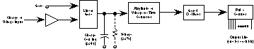
LeCroy 2249 Series and 2259B ADCs measure either charge or voltage using the Wilkinson
charge run-down technique. A block diagram of an ADC employing charge run-down is shown in
Figure 1.
Figure 1
The input to the ADC is sampled and the result is stored as charge on a capacitor. After a
short interval, the capacitor is discharged at a constant rate, producing a time
proportional to the input charge. The time is meas ured by counting the number of
oscillator pulses during the discharge interval.
The Model 2249A contains twelve complete ADCs in a single-width CAMAC module. Each ADC
offers a resolu tion of ten bits to provide 0.1% resolution over a wide 1024-channel
dynamic range. The input sensitivity of the Model 2249A is 0.25 pC/count for a full scale
range of 256 pC. This is compatible with most available signal sources and no additional
buffering or reshaping of any kind is required to digitize nanosecond pulses.
The excellent long-term stability, temperature characteristics, and isolation between ADC
channels assure accurate and reliable performance. Confirmation of operation and
calibration is provided by the test feature which allows all twelve ADCs or an entire
system to simultaneously digitize a charge proportional to a DC level provided to a
front-panel Lemo connector or patched into P1, P2, or P5 of the Dataway connector.
The Model 2249A offers excellent event rate capability through the incorporation of a fast
clear and a fast digitizing rate. The fast clear input enables the ADC to begin digitizing
on the command of a prompt gate and be reset, if necessary, before the end of conversion
on the basis of delayed logic or chamber information.
End of conversion of modules which contain data is flagged by generation of a CAMAC LAM.
Readout of modules which do not contain information can be eliminated either by use of the
LAM signals or through Q suppression.
The Model 2249SG is a separately gated version of the 2249A, in a double-width CAMAC
module. A separate START gate is also required, which must be applied at approximately the
same time as the first of the separated gates. A fixed time (~ 2 �sec) after the START
pulse all channels convert.
The Model 2249W is an 11-bit integrating-type analog-to-digital converter. It has been
optimized for linearity and stability, and allows operation at wide gates of up to 10
�sec. Thus, the 2249W is compatible with CsI and Nal crystal detectors. The minimum gate
of 30 nsec makes its use with organic scintillators and Cerenkov detectors possible in all
but the highest rate conditions.
By AC-coupling the input, 11-bit (1980 counts) operation has been achieved with �2 count
integral linearity. This linearity is maintained from the smallest signal size to signals
as large as -2 V.
The Model 2259B is also based on the design of the Model 2249A. Digital sections are
identical, utilizing the same synchronized oscillator circuit and low-power LeCroy Model
SC100 Hybrid scaler section. The analog front end of the 2259B employs the LeCroy Model
VT100C Voltage-to-Time Converter.
The 2259B accepts negative-going analog inputs up to -2 V in amplitude within its linear
dynamic range, giving an 11-bit digital output proportional to the peak of the pulse
falling within an externally applied gate interval. The resultant ADC sensitivity is
approximately -1 mV/count. The analog input signal should have at least a 50 nsec rise
time. Because of the nature of the peak detector, the 2259B is insensitive to the fall
time of the input pulse. The minimum recommended gate duration is 100 nsec, and should
enclose the negative peak of the input pulse. Gate widths up to 5 �sec may be employed.
Digitizing time of the 2259B is fixed at approximately 106 �sec.
Analog Inputs: Twelve; Lemo-type connectors; charge-sensitive (current-integrating);
direct-coupled, quies cently at approximately +4 mV; 50 ohm impedance; linear range
normally -2 mV to -1 V; protected to �50 V against 1 �sec transients.
Full Scale Range: 256 pC �5%.
Full Scale Uniformity: �5%.
Integral Non-linearity: �0.25% of reading �0.5 pC (12 pC to 256 pC) for > 500
ohm source.
ADC Resolution: 10 bits actual, (0.1%).
Long-Term Stability: Better than 0.25% of reading �0.5 pC/week (at constant
temperature).
Temperature Coefficient: Typical, 0; max., �[.03% of reading (in pC) + .002 t]
pC/�C (where t = gate duration in nanoseconds, with 50 ohm reverse termination).
ADC Isolation: A 5 V, 20 nsec overload pulse in any one ADC disturbs data in any
other ADC by no more than 0.25 pC.
Gate Input: One gate common to all ADCs; Lemo-type connectors; 50 ohm impedance;
NIM levels (-600 mV or greater); minimum duration, 10 nsec; maximum recommended duration,
200 nsec (actual limit approximately 2 �sec with reduced accuracy; partial analog input
must occur within 0.5 �sec after opening gate to preserve accuracy), effective opening
and closing times; 2 nsec; internal delay, 2 nsec.
Fast Clear: One front-panel input common to all ADCs; Lemo-type connector; 50 ohm
impedance; -600 mV or greater clears, minimum duration, 50 nsec. (Caution: narrower pulses
cause partial clearing.) Requires additional 2.0 �sec settling time after clear.
Residual Pedestal: Typically 1 + 0.03t pC (where t = gate duration in nanoseconds)
with 50 ohm reverse termination.
Test Function: With CAMAC I present, the positive DC level applied to front panel
"Test" input (internal high impedance connection to +12 V) or optional rear
connector P1, P2, or P5 patch points will inject charge with a proportionality constant of
-12.5 pC/V into all inputs at F(25) � S2 time. (With CAMAC I not present F(25) � S2 will
generate the 80 nsec gate only, providing a measure of residual pedestal only.)
Conversion Time: 60 �sec. By factory option, 8-bit operation at 12.5 �sec
digitizing time may be provided.
Q and LAM Suppression: Adjustable potentiometer (accessed from side of module) sets
count level required (from 0 to 100) before data is considered useful. A module in which
all channels contain less than set amount will produce no Q response or LAM and appears
during readout as an empty CAMAC slot, thus reducing readout time. A Command Accepted
response is still generated. The LAM suppress portion can be disabled with a solder jumper
option.
Packaging: CAMAC #1 module.
Current Requirements: +24 V at 35 mA; -24 V at 15 mA; +6 V at 850 mA; -6 V at 200
mA.
Analog Inputs: Twelve; Lemo-type connectors; charge-sensitive (current-integrating);
direct-coupled, quies cently at approximately +4 mV; 50 ohm impedance; linear range
normally -2 mV to -1 V; protected to �50 V against 1 �sec transients.
Full Scale Range: 256 pC �5%.
Full Scale Uniformity: �5%.
Integral Non-linearity: �0.25% of reading �0.5 pC for > 500 ohm source.
ADC Resolution: 10 bits (0.1%) somewhat degraded to approximately 0.2% by clock
unsynchronized with any specific linear gate input.
Long-Term Stability: Better than 0.25% of reading �0.5 pC/week (at constant
temperature).
Temperature Coefficient: Typical, 0; max., �[.03% of reading (in pC) + .002 t]
pC/�C (where t = gate duration in nanoseconds, with 50 ohm reverse termination).
ADC Isolation: A 5 V, 20 nsec overload pulse in any one ADC disturbs data in any
other ADC by no more than 0.25 pC.
Gate Input: Twelve, one per ADC; Lemo-type connectors; 50 ohm impedance; NIM level
> 600 mV; minimum duration, 10 nsec; maximum recommended duration, 200 nsec (actual
limit approximately 2 �sec with reduced accuracy; partial analog input must occur within
0.5 �sec after opening gate to preserve accuracy), effective opening and closing times; 2
nsec; internal delay, 2 nsec. All gates should occur within 2 �sec of the
"start" pulse (other arrangements require internal resistor change). CAUTION:
Subsequent gate signals are NOT INHIBITED after receipt of the first one, so care must be
taken to externally prevent the application of more than one gate to each channel until a
clear is applied.
Start Input: A NIM level (> -600 mV) signal of a duration exceeding 10 nsec must
be applied to start the internal oscillator. It should be applied simultaneous to the
earliest gate pulse or should follow it by no more than 100 nsec.
Fast Clear: One front-panel input common to all ADCs; Lemo-type connector; 50 ohm
impedance; -600 mV or greater clears, minimum duration, 50 nsec. (Caution: narrower pulses
cause partial clearing.) Requires additional 1.5 �sec settling time after clear.
Conversion Time: 60 �sec.
Q and LAM Suppression: Adjustable potentiometer (accessed from side of module) sets
count level required (from 0 to 100) before data is considered useful. A module in which
all channels contain less than set amount will produce no Q response or LAM and appears
during readout as an empty CAMAC slot, thus reducing readout time. A Command Ac cepted
response is still generated. The LAM suppress portion can be disabled with a solder jumper
option.
Packaging: CAMAC #2 module.
Current Requirements: +24 V at 35 mA; -24 V at 15 mA; +6 V at 850 mA; -6 V at 200
mA.
Analog Inputs: Twelve; Lemo-type connectors; charge-sensitive (current-integrating);
AC-coupled (2 msec time constant, field changeable); 50 ohm impedance; linear range
normally 0 to -2.0 V; protected to �50 V against 1 �sec transients.
Gain: -0.25 pC/count �5%.
Full Scale Range: Approximately -500 pC (maximum count @ 1980).
Integral Non-linearity: �0.05% �(0.5 pC +0.1%).
ADC Resolution: A 5 V, 20 nsec overload pulse in any one ADC disturbs data in any
other ADC by no more than 0.5 pC (2 counts).
Gate Input: One gate common to all ADCs; Lemo-type connectors; 50 ohm impedance;
-600 mV or greater enables; minimum duration, 30 nsec; maximum recommended duration up to
10 �sec; partial analog input must occur within 0.5 �sec after opening gate to preserve
accuracy, effective opening and closing times; 5 nsec; internal delay, 7 nsec.
Fast Clear: One front-panel input common to all ADCs; Lemo-type connector; 50 W
impedance; -600 mV or greater clears, minimum duration, 50 nsec. Requires additional 2.0
�sec settling time after clear.
Pedestal: Adjustable over approximately 100 counts via side-panel accessed trimmer
capacitor. Somewhat higher for wide gate.
Test Function: With CAMAC I present, the positive DC level applied to front panel
"Test" input (internal high impedance connection to +12 V) or optional rear
connector P1, P2, or P5 patch points will inject charge with a proportionality constant of
-15 pC/V into all inputs at F(25) � S2 time. (With CAMAC I not present F(25) � S2 will
generate the gate only, providing a measure of residual pedestal.)
Conversion Time: 106 �sec.
Q and LAM Suppression: Adjustable potentiometer (accessed from side of module) sets
count level required (from 0 to 100) before data is considered useful. A module in which
all channels contain less than set amount will produce no Q response or LAM and appears
during readout as an empty CAMAC slot, thus reducing readout time. A Command Ac cepted
response is still generated. The LAM suppress portion can be disabled with a solder jumper
option.
Packaging: CAMAC #1 module.
Current Requirements: +24 V at 143 mA; -24 V at 75 mA; +6 V at 725 mA; -6 V at 155
mA.
Analog Inputs: Twelve; Lemo-type connectors; voltage (peak) sensing; direct-coupled,
quiescently at approximately +0.5 mV; 50 ohm impedance; protected to �100 V against 1
�sec transients; accepts either negative-going pulses of 50 nsec rise time or bipolar
pulses with negative lobe first.
Gain: (1 �0.05) counts/mV.
Full Scale Uniformity: �5%.
Integral Linearity: �(0.1% + 1 count) from 7% to 100% of full scale.
ADC Full Scale: 2020 �20 counts, -2 V �5%.
Long-Term Stability: Better than 0.25% of reading �4 mV/week (at constant
temperature).
Temperature Coefficient: Typical 0; maximum, �0.03%/�C of full scale.
ADC Isolation: A -5 V, 100 nsec overload pulse in any one ADC disturbs data in any
other ADC by no more than 5 mV.
Gate Input: One gate common to all ADCs; Lemo-type connectors; 50 ohm impedance;
-600 mV or greater enables; minimum duration, 100 nsec; maximum recommended duration, 5
�sec; effective opening and closing times; 2 nsec; internal delay, 5 nsec; must enclose
negative peak of input pulse; pulse position dependence within the gate < 2 counts
/�sec.
Fast Clear: One front-panel input common to all ADCs; Lemo-type connector; 50 ohm
impedance; -600 mV or greater clears, minimum duration, 50 nsec. (Caution: narrower pulses
cause partial clearing.) Requires additional 2 �sec settling time after clear.
Pedestal: 35 �25 counts with dependence on gate width < 2 counts/�sec.
Test Function: With CAMAC I present, the positive DC level applied to front panel
"Test" input (internal high impedance connection to 10 V) or optional rear
connector P1, P2, or P5 patch points will inject signal with a proportionality constant of
-0.167 V/V into all inputs at F(25) � S2 time. (With CAMAC I not present F(25) � S2 will
generate the 100 nsec gate only, providing a measure of residual pedestal only.)
Conversion Time: 106 �sec.
Q and LAM Suppression: Adjustable potentiometer (accessed from side of module) sets
count level required (from 0 to 200) before data is considered useful. A module in which
all channels contain less than set amount will produce no Q response or LAM and appears
during readout as an empty CAMAC slot, thus reducing readout time. A Command Ac cepted
response is still generated. The LAM suppress portion can be disabled with a solder jumper
option.
Packaging: CAMAC #1 module.
Current Requirements: +24 V at 35 mA; -24 V at 15 mA; +6 V at 850 mA; -6 V at 200
mA.
All models will generate an X = 1 (command accepted) response to any valid F, A, and N
command. In addition, a Q = 1 response is generated in recognition of a F(0) or F(2) Read
function or an F(8) function if a Look-At-Me (LAM) has been set. There will be no response
(Q = 0) under any other condition. A LAM signal is generated from end of conversion until
a module Clear or Clear LAM has been asserted. The LAM signal can be permanently enabled
or disabled by the appropriate CAMAC function code, and can be tested by Test LAM.
Standard option causes LAM to be suppressed for empty modules. In addition, an adjustable
potentiometer (accessed from side of module) sets count level required (0 to 100 for the
2249 Series and 0 to 200 for the 2259B) before data is considered valid. A module in which
all channels contain less than the set amount will produce no Q-response or LAM and
appears as an empty CAMAC slot during readout, thus reducing readout time. The LAM
suppress portion can be disabled with a solder jumper option.
Unless otherwise noted, the 2249 Series of ADCs along with the 2259B ADC respond to the
following CAMAC command and function codes.
CAMAC COMMANDS
C or Z: ADCs and LAM are cleared by the CAMAC Clear or Initialize command.
I: Gate input is inhibited during CAMAC Inhibit command (see Notes 1, 2, 3, and 4).
CAMAC FUNCTION CODES
F(0): Read registers; requires N and A. A(0) through A(11) are used for channel
addresses.
F(2): Read registers and clears module and LAM; requires N and A: clear on A(11)
only.
F(8): Test LAM; requires N and any A from A(0) to A(11) independent of Disable LAM.
Q response is generated if LAM is set.
F(9): Clear module and LAM; requires N, and any A from A(0) to A(11).
F(10): Clear LAM; requires N, and any A from A(0) to A(11).
F(24): Disable LAM; requires N, and any A from A(0) to A(11).
F(25): Test module; requires N, and any A from A(0) to A(11). See Notes 1, 2, 3,
and 4.
F(26): Enable LAM; requires N, and any A from A(0) to A(11). Remains enabled until
Z or F(24) applied.
Caution: The state of the LAM mask will be arbitrary after power turn-on.
Notes
1. With CAMAC I present, the positive DC level applied to front-panel "Test"
input of the 2249A or optional rear connector P1, P2 or P5 patch points will inject charge
with a proportionality constant of -12.5 pc/V into all inputs at F(25)�S2 time. With
CAMAC I not present, F(25) will generate a gate of approximately 80 nsec, providing a
measure of residual pedestal only.
2. The 2249SG does not respond to F(25) and has no test feature. However, on-line test
capability is optional at the expense of CAMAC Inhibit with Q7 (the "inhibit"
transistor) removed, the leading edge of a pulse applied to the START input will cause a
fixed charge to be injected onto the 2249SG analog inputs. Coincident with the START, the
12 gate pulses must be applied for a duration of approximately 80 nsec. Proportionality
constant is -12.5pC/V of DC signal level applied to P1, P2, or P5 patch points for an 80
nsec gate. In this test mode, the gates must precede the START by 10 nsec. CAUTION: If
this test feature is implemented, then the CAMAC I is non-functional.
3. The test feature of the 2249W is the same as the 2249A except that the proportionality
constant becomes -20 pC/V.
4. The test feature of the 2259B is the same as the 2249A except that the proportionality
constant becomes -167mV/V.
Table Notes
1. Protected to �50 V (+100 V/2259B) against 1 �sec transients.
2. Partial analog input must occur within 0.5 �sec after gate opening.
3. Effective opening and closing times 2 nsec; internal delay 2 nsec (2249A, 2249W) or 5
nsec (2259B).
4. Requires 2 nsec settling time.
5. Must include negative peak of input pulse. Dependence of position of pulse within the
gate: < 2 counts/�sec.
6. Must proceed inputs signal by at least 20 nsec.
* Included for completeness. See separate data sheet for details.
Copyright� September 1995. LeCroy is a registered trademark of LeCroy Corporation. All
rights reserved. Information in this publicaction supersedes all earlier versions.