The Model VV100B is a wide bandwidth, gain-of-10 pulse amplifier packaged
as a standard 16-pin DIP hybrid circuit. Representing a major advance in
fast amplifier bandwidth, stability, dynamic range, and general utility,
the VV100B provides unprecedented performance in demanding direct-coupled,
high-duty-cycle applications.
An ideal "transparent gain" element would simply magnify the input
signal without significant distortion of operat ing constraints. The VV100B
performance is very close to this ideal by virtue of its extraordinary stability,
speed, linearity, and noise characteristics.
A high-speed amplifier circuit design makes the performance of the VV100B
virtually independent of external variables such as supply voltages or temperature.
Shifts in the DC output level remain negligible even when the amplifier
is subjected to extremes of operating temperature of variations in power
supplied. There is virtually no warm-up drift at turn-on.
The Model VV100B is a hybrid circuit designed as a high bandwidth amplifier
primarily intended for amplification of negative pulses such as those from
photomultiplier tubes. It has a fixed gain of 10 and a rise time of less
than 2 nsec. The output is capable of driving two 50 ohm loads (25 ohm).
The linear range of the VV100B is +200 mV to -5 V.
The user may supply suitable input impedance for his particular needs. The
unit requires an input terminating resistor, power supply bypass capacitors,
input and output DC trims and an output shape capacitive trim.
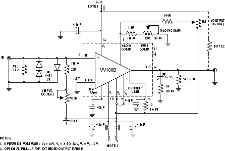
Figure 1 show a typical application circuit for the VV100B and is the circuit
on the LeCroy VV100BTB amplifier. Here input trim T1 is accomplished by
the series combination of a 27 kohm resistor and a 500 kohm potentiom eter.
Trim T2 is set by the 1 Mohm potentiometer and series 100 kohm fixed resistor.
A fixed resistor to ground sets the low frequency gain trim (T3). High frequency
compensation is set by the 51 ohm, 6-35 pF combination.
The VV100B contains output protection circuitry which limits the average
output current to 60 mA. The time constant of the limiting circuit is approximately
6 µsec.
The internal current limiting of the VV100B is defeated by placing a jumper
between Pins 13 and 2. This connec tion allows bipolar operation if an additional
resistor is connected from the output to the positive supply voltage V 1.
All positive current delivered to the load is through this additional resistor.
The DC value of this added current should be held to less than 40 mA.
If internal current limiting is not defeated, the maximum positive voltage
excursion into a load R L is:
V+max = V1 / RP + RL
The most negative will be given by:
V-max = -RL [0.06 RL + V1] / RL + RP
Because of the extremely high bandwidth of the VV100B, care should be used in layout of the printed circuit board. Continuous ground plane construction is essential. To ensure minimum inductance, low profile sockets should be used. Insertion pins (Berg 75315-001 or equivalent) are even better. Input busses should be separated from the output. Interconnections to other circuitry greater than 3 cm away should be made only by properly terminated coaxial cable. Input protection circuitry and bypass capacitors should be located as close to the hybrid as possible.
Proper termination and protection must be supplied to the input. In most
cases, input to the amplifier will be via 50 W cable. In this case, a 50
ohm resistor from the input (pin 8) to ground should be employed. In addition,
three 1N4448 or equivalent diodes to ground as shown in Figure 1 will provide
overload protection. The input DC level must be trimmed to zero by a trim
resistor (T1) to a negative supply. Where the best DC stability is required,
this supply should be regulated. Note that fluctuations in the input offset
will appear at the output amplified 10 fold.
Figure 1
A current of about 30 mA from +6 V must be supplied at Pin 12. In addition, two negative supplies, V 2 and V3 are recommended. V2 (Pin 2) requirement is 20 mA at a voltage between -6 and -12. V 3 (Pin 10) is to be set 12 V more negative than V2. For example, with V 2 set to -12 V, V3 should be -24 V. The VV100B requires about 8 mA from the V3 supply. Proper bypass requires at least 6.8 µF tantalum capacitors to ground from Pins 2, 12, (and 10 if three voltages are used) and 47 µF on Pin 6. Minimum length leads should be employed. Be sure to observe proper polarity. See Figure 1. Model VV100B can be operated with only two power supplies at the expense of rise time and linearity. For this configuration, tie Pin 2 to Pin 9, set V 2 = -6 V to -12 V, V3 is omitted and V1 = +6 V.
The VV100B is optimized for a 25 ohm load in order to drive two 50 ohm cables simultaneously. If only one cable is to be driven, a 50 ohm resistor should be connected from the output of the VV100B to ground, to provide a net 25 ohm load. Other cable impedances may be driven, taking care to maintain the required 25 ohm through the use of additional series or shunt resistance. For example, three 91 ohm cables require an additional 142 ohm shunt to ground; five 50 ohm cables may be driven via five 75 ohm series resistors (yielding reduced gain and output swing as the price of the additional fan-out). Driving loads other than 25 ohm will cause output shape and stability problems. Loads less than 25 ohm degrade rise time, gain, and linear range; loads larger than 25 ohm produce ringing and oscillation.
The output of the VV100B is protected against sustained shorts to ground
in the presence of DC inputs. This short circuit protection is implemented
by an integrating stage which senses output current and limits it to an
average current of 60 mA. The time constant of the limiting stage is approximately
6 µsec. The maximum pulse output current is a function of the input
pulse width, amplitude and repetition rate.
When limiting occurs, this integrating stage must recover before linear
operation resumes. Longer averaging times can be achieved by adding capacitance
from Pin 13 to ground. Current limiting may be defeated by a jumper from
Pin 2 to Pin 13. Under this condition, safe operation requires (V out -
V2) iout < 1 W.
The limiting circuitry is based on the average output current of the VV100B.
The maximum output swing for pulses less than the averaging time is:
dmax = (60 mA) / D
Here D is the duty factor. For larger widths the VV100B output begins to shut down and approach 60 mA with a 6 µsec time constant.
The VV100B requires three separate trims; input DC level, output DC level
and fast compensation*. The values of these trims must be selected for each
VV100B and hence must be reset if the VV100B is replaced. All trims should
be made with the VV100B output loaded with 25 ohm.
* Occasionally an additional slow compensation trim (T3) is required.
To make this trim, a flat-topped pulse of about 10 µsec duration is
applied to the VV100B input. A resistor in the range of 10 kW to 300 kW
connected from pin 1 to pin 4 (or ground as required) is used to trim the
output pulse to a flat top.
The first trim, T1, is used to set the input DC offset. With no input to
the VV100B, install a resistor between the input connector and a regulated
negative supply. The value of the resistor should be chosen to set the input
voltage to 0.0 mV. Typical values of this trim are 30 kohm to 300 kohm.
The second trim, T2, is used to set the output DC level to zero. This trim
is a resistor from Pin 1 to either the negative or positive supply, depending
upon the polarity of the initial DC offset. Typical values of this trim
are 100 kohm to 1 Mohm.
The last trim is an RC adjustment to the overshoot of the output. A 6-35
pF trimmer capacitor in series with a 25 -100 ohm resistor is required to
minimize the overshoot. Using a fast rise time input pulse, observe the
output of the VV100B. Adjust the trim capacitor to give the best output
pulse shape.
Gain: 10 fixed, ±5% tolerance, non-inverting, long term
stability ±1%.
Linearity: ±0.2% integral (0 to -3 V).
Maximum Output Swing: 5 V at 200 mA (Note 1); +250 mV at 5 mA (Note
3).
Output Impedance: < 0.2 ohm for negative outputs.
Frequency Response: Full signal bandwidth (3 dB) is 170 MHz for 2
voltage operation (Notes 4 & 7); 200 MHz for 3 voltage operation.
Rise Time: 2 nsec (10% to 90%).
Input Signal Range: Maximum safe input signal is ±1 V; external
clamp diodes recommended (Note 6). Linear range is -0.5 V to +0.01 V.
Wideband Output Noise: < 50 µV R.M.S. (referred to input).
Input Impedance: > 1 kohm.
Input Bias Current: -25 µA; drift vs. temperature 250 nA/°C.
Input Offset Voltage: 2 mV, adjustable to 0 typical; drift vs. temperature
10 µV/°C (max.); drift vs. supply voltage < 100 µV, for
±1% variation; drift vs. time < 100 µV, long term.
Coupling: Input and output are DC-coupled.
Temperature Range: 0°C to 70°C.
Power Supply Rejection Ratio: 90 dB at 120 Hz.
Power Supply: Two voltage operation (Note 4). Rated voltage, quiescent,
V 1 = 30 mA at +6 V. Current, V2 = -20 mA at -6 V to -12 V; (tie Pin 9 to
Pin 20).
Power Supply: Three voltage operation (Note 5). V 1 = 30 mA at +6
V; V2 = -28 mA at -6 V to -12 V; V3 = 8 mA at V2 - 12 V (e.g., -24 V when
V2 = -12 V and Pin 9 open).
Overload Recovery: Operation with V2 = -12 V supply, saturated for
approximately 15 nsec after 10 x overload.
Package: Standard 16-pin dual in-line hybrid integrated circuit.
(Note 8).
Notes
1. Overload protected to limit the average output current to < 60 mA.
See application notes.
2. No overload protection. Average output current should be < 50 mA to
avoid damage to the unit.
3. For increased positive swing, see applications notes.
4. Three voltage operation recommended for most applications.
5. Three voltage operation provides increased bandwidth.
6. See Figure 1.
7. For two voltage operation install a 6.8 µF capacitor from Pin 13
to ground with the positive lead grounded.
8. The VV100B is not pin-for-pin compatible with the VV100. Please contact
LeCroy for details.
Ordering Information
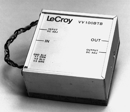
The Model VV100BTB provides the high bandwidth circuitry, shown in Figure
1, in a ready-to-use format. The 3 inch x 3 inch x 1.6 inch enclosure size
of the device allows one to use the Model VV100B in locations too small
for many fast amplifiers. The amplifiers employ Lemo type coaxial cable
connectors. The units may be purchased with a Model VV100B. The trim and
compensation variables are factory adjusted for optimum high-speed perfor
mance.
Model Description
VV100B: Amplifier hybrid.
VV100BTB: VV100B mounted in circuit board. Lemo connectors.
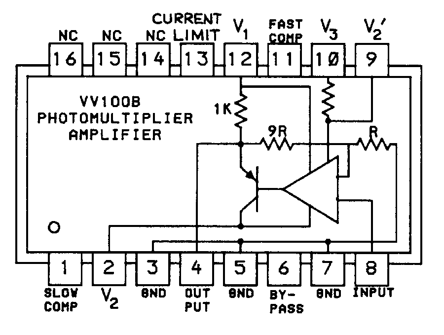
Logic Diagram (Top View)
Model VV100BTB Wideband Amplifier Module
Copyright© July 1997. LeCroy is a registered trademark of LeCroy Corporation.
All rights reserved. Information in this publicaction supersedes all earlier
versions.