When logical addressing is enabled use top configuration.
When logical addressing is disabled use bottom configuration.
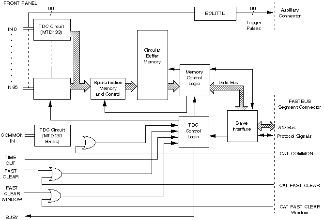
The FASTBUS Model 1877S is a 96-channel, high resolution, multihit TDC designed for high
rate experiments. This TDC provides precise time measurements for spectrometers and
hodoscopes consisting of multiwire propor tional, drift or time projection chambers. With
a least count of 500 psec and a 16-bit range, the Model 1877S can measure time intervals
up to 32 Ásec duration. The instrument operates in Common Start or Common Stop modes.
Common Stop Mode eliminates the need for expensive delay cables normally required for each
input channel of a fixed target experiment.
The 1877S provides the high performance, high density, versatility, and automated test
features required for large scale experiments. By using the FASTBUS standard, the LeCroy
1800 family of data acquisition modules is one of the most sophisticated data acquisition
systems today.
The individual channel inputs are located on the front panel. They accept differential ECL signals and are termi nated in 110 W. The COMMON input (Common Start or Stop) also accepts ECL signals and has a removable 110 ohm termination. By removing this termination, the COMMON signal(s) can be cascaded, as long as the termination in the last module of a block of modules is left in place. This scheme eliminates the extra propagation delays caused by embedded repeaters and leaves only the very slight delays due to the cables cascading the individual modules (approximately 50 psec/cm).
At the heart of the 1877S lies the MTD133B Monolithic Time Digitizer, an 8-channel,
16-bit dynamic range TDC circuit with 500 psec least count. Arrival times can be recorded
for either the rising, falling or both edges. The double pulse resolution is 20 nsec.
The MTD133 uses a high-speed clock, a continuously counting scaler, and a three state
interpolator. When a pulse arrives, the contents of the scaler and interpolator are stored
in memory. Up to 16 words of data can be stored in the LIFO (Last In First Out memory) for
each channel. During readout each of the stored signal times is automatically subtracted
from the COMMON hit time. Therefore, the output is the actual time difference with
virtually no pedestal. The difference value is further compared to a programmable upper
threshold and discarded if it is greater than this threshold. This threshold is
programmable from 8 nsec to 32 Ásec with a resolution of 8 nsec.
In this way the MTD133 accommodates many different, difficult measurement scenarios. For
users who wish to detect only pulses coming within the drift time of the chamber, the
programmable threshold produces a program mable full scale. In addition, the user can
program the depth of the LIFO from 1 to 16 hits, thus creating a guaran teed maximum
conversion time.
Model 1877S Block Diagram
Control registers configure the TDC to report either the time of the rising edges, falling edges or both, facilitating pulse width measurements. Test functions allow verification of each channel's behavior. Full scale time out in the COMMON START mode can either be programmed or supplied externally. Compatibility with the Model 1810 Calibration and Timing Module is maintained for COMMON START/STOP, fast clear, fast clear window, and test pulse distribution.
The module contains an eight event buffer. This digital memory buffer provides two primary advantages. First, dead time in the experiment is reduced because data readout can be done during the acquisition of subsequent events. Second, the event data can be stored temporarily while the trigger decision to read or discard the event is made. Events in the buffer are discarded with a FASTBUS command to skip the event. This skip command causes an internal pointer to increment, positioning the next event at the top of the readout queue. As each event is recorded, a modulo eight event tag number is appended to it in order to allow the coherence across multiple modules to be verified.
The 1877S complies with the FASTBUS Standard (ANSI/IEEE-960). FASTBUS functions allow
remote control and operation of the 1877S. Data from the 1877S is automatically zero
suppressed. Readout is in a FIFO-like manner, consisting of a header word followed by a
variable number of data words. Channel identification informa tion is appended to each
data word.
The modules may be read out via a LeCroy Model 1821 FASTBUS Segment Manager/Interface
(SM/I) at data transfer rates up to 10 Mwords/sec. In addition, the Model 1877S is
compatible with the LIFT (LeCroy Interactive FASTBUS Toolkit) software package.
The 1877S provides the features necessary for interface and readout of single and
multi-range charge-to-time converting front ends. The 1877S then provides the time
encoding function and FASTBUS readout of the charge signal. The charge-to-time converters
always generate an output pulse, even at pedestal so that non-zero time data is recorded
by the 1877S on every channel. By being able to encode both input edge polarities, widths
of pulses can be encoded.
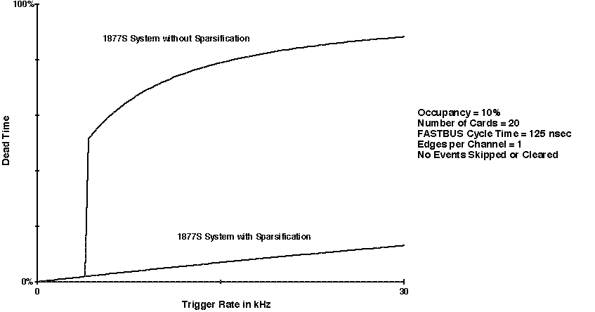
In a mode similar to the LeCroy Model 1881M, a sparse data readout scheme can be used to
prevent unwanted data from being buffered. The 1877S allows the user to program 96
constants, one per channel, which can be compared to the measurement values. Data
exceeding these individual thresholds is buffered reducing both the dead time and quantity
of data that must be transferred over FASTBUS to the host computer. See Figure 1.
Figure 1
When the 1877S is used in a multi-range ADC application (e.g. MQT300), the TDC is
programmed to operate in Common Start mode. The Common Start timeout (as appropriate for
the desired full scale and resolution) can be selected by configuration at the TDCs CRSs.
A two bit hit count field has been provided in the 1877S data word format. This indicates
(modulo 4) how many hits were recorded in the channel's LIFO. By using the FASTBUS
controlled readout depth parameter it is pos sible to readout only 1 word per channel,
while also knowing the total number of hits on that channel. This feature provides a
second level of data reduction from the multi-range MQT300 so that only 1 data word per
channel is necessary.
Inputs: 96 ECL differential line receivers. Input impedance 110 ohm ▒10%.
Minimum pulse width 10 nsec FWHM (must be > 1 time bin width). Input swing 400 mV,
differential.
Least Significant Bit: 500 psec.
Total R.M.S. Error: 400 psec (Note: The R.M.S. of a gaussian distribution is equal
to sigma).
Time Out: Differential ECL input to mark the end of acquisition in COMMON START
mode.
Full Scale: 0 to 32.768 Ásec, ▒0.0025%; programmable via CSR18 in steps of 8
nsec.
Pedestal: 14 to 20 counts.
Double Edge Resolution: The 1877S can measure two edges separated by as little as
10 nsec. No two pulse edges should be closer than 10 nsec. This implies a lower limit on
the double pulse resolution of 20 nsec.
Common Start/Stop: From the Model 1810 CAT via TR6 line or from front-panel
differential ECL input. CSR selected.
Fast Clear Window Input: From the Model 1810 CAT via TR5 line.
Fast Clear Window (FCW): Starts at end of Time Range (Common Start) or at Common
Stop. Can be pro grammed 1024 nsec to 512 Ásec. During this period, the user can apply a
FAST CLEAR to discard the event just captured.
Zero Suppression: Automatic for channels that have no hit.
Long Term Stability: < 100 ppm/year.
Temperature Coefficient: < 10 ppm/░C.
Differential Non-Linearity: Maximum ▒0.2 LSB.
Integral Non-Linearity: < 25 ppm full scale.
Fast Clear: Differential ECL input via a 2-pin front-panel connector (removable
termination resistors) or via backplane TR0 line. Minimum pulse width 40 nsec.) When
applied during the FCW, clears data in the current event and readies module for acceptance
of a new event. Fast clear settling time is < 250 nsec. Fast Clear is leading edge
sensitive and must be performed during FCW.
Time Out: Differential ECL input via a 2-pin front-panel connector. Minimum width
50 nsec. In Common START mode, terminates measurement in progress and starts conversion.
Busy Output: Differential ECL output via a 2-pin front-panel connector. Indicates
the module is converting hit information. The unit is unavailable for data capture.
Conversion Time: 1.2 Ásec + 50 nsec per hit within the programmed full scale; 1.75
Ásec minimum.
On-Board Tester: The tester generates square wave pulses (50% duty cycle). The
pulse trains can have 1, 2, 4 or 8 cycles with half periods of 125, 250, 1000 nsec or 2000
nsec.
Multiple Event Buffer: The digital data memory is logically organized as a circular
buffer, large enough to store the results of up to eight events.
Front-Panel Indicators: Slave: Indicates module is being addressed. COMMON:
Indicates whether Common Start/Stop was hit.
Power Requirements: 4.0 A at 5 V; 7.7 A at -5.2 V; 3.1 A at -2 V; 0.1 A at +15 V;
0.1 A at -15 V.
Packaging: Single-width FASTBUS module (ANSI/IEEE-960-1989).
Module Identification Code: Read Only, 103D h.
Implemented Addressing Modes: Logical (16 bits), Geographical, Broadcast.
AS-AK Handshake Time: 125 nsec typical, 150 nsec maximum.
DS-DK Handshake Time: 65 nsec typical, 75 nsec maximum (Block Transfer).
Implemented Broadcast Functions:
Code Significance Comments
(01)h* General Broadcast Select The TDC modules are selected and respond to subsequent
data cycles.
(05)h Class N Broadcast The TDC modules of Class N (programmed via CSR7) respond to
subsequent data cycles.
(09)h Sparse Data Scan TDC modules containing one or more buffered events assert (SDS)
their "T pin" on the following read data cycle.
(19)h Device Available Scan TDC modules respond by asserting "T pin" if no
events are (DAS) buffered.
(0D)h All Device Scan All TDC modules assert their T pin on the following read
data cycle.
(CD)h TDC DS TDC modules assert T pin if current event contains a non-zero
number of data words.
* An h subscript denotes a hexadecimal number, i.e., base 16.
Module Control Space Registers
CSR 0h Module ID and control/status
CSR 1h Mode and control
CSR 3h Logical address
CSR 5h Block transfer word count register
CSR 7h Broadcast class
CSR 10h Buffer memory page pointers
CSR 12h Full scale time measurement
CSR C0000000h Sparsification constants, one per channel
- CSR C000005Fh
Slave Status Responses to Data Cycles
SS Significance
0 Valid action.
2 End of data.
3 Error: Error in token pass during multi-module data scan.
7 Error. Invalid secondary address loaded into internal address register.
When logical addressing is enabled use top configuration.
When logical addressing is disabled use bottom configuration.
![]()
![]()
D = Data
S = Edge: Rising Edge = 0, Falling Edge = 1 (on "+" inputs)
A = Channel number 0 - 95
G = Geographic address
L = Logic address
P = Parity
W = Word Count
H = MTD133 Hit Count
Copyright® March 1997. LeCroy is a registered trademark of LeCroy Corporation. All
rights reserved. Information in this publicaction supersedes all earlier versions.