The Fast Encoding and Readout ADC (FERA) and Fast Encoding and Readout TDC (FERET) systems
consist of modules designed for fast conversion of analog information, either charge or
time intervals, into a digital format. They also provide fast readout to a storage memory
module or to a computer for further processing. The system modularity allows small as well
as large multi-channel ADCs or time digitizing (TDC) systems to be configured and also
allows simple memory expansion. These units can be used with other modules to configure
energy or time based triggers tailored for specific applications.
The heart of the system is the Model 4300B, a charge sensitive analog-to-digital
converter. Other elements in the system include the Model 4301, a utility module for
distribution of common signals and regeneration of signals for multiple 4300Bs; the Model
4302, a dual port fast access memory module; and the Model 4303, which converts time
intervals into charge signals to be measured by the Model 4300B.
Constant Short Conversion Time - The time for conversion is 4.8 Ásec at 10 bits
and 8.5 Ásec at 11 bits. This is independent of the number of channels or modules making
up a system.
Fast Data Readout - A readout speed of 10 megawords/sec, associated with pedestal
subtraction and zero suppression capabilities, allows a uniquely fast data acquisition
rate both for charge and time interval measure ments.
High Resolution - The least count resolution in charge is 0.25 pC. It is adjustable
in time from 50 psec to 500 psec.
Expandable Memory - Data can be stored in cascadable, 16 kiloword deep memory
modules.
System Flexibility - Due to its modular nature, a system can be easily expanded and
adapted to measure charge or time intervals or both, and can also be easily interfaced to
CAMAC, FASTBUS or GPIB.
Trigger Capability - The FERA/FERET systems have been designed so that the
digitized charge or time informa tion can be given as an input to second level trigger
processors built around the ECLine Data Handler Modules.
A Fast Encoding and Readout ADC (FERA) system includes the Model 4300B and may also
include additional accessory modules such as the Model 4301 FERA Driver and/or the Model
4302 Dual Port Memory.
A Fast Encoding and Readout TDC (FERET) high resolution system always includes the Model
4300B and the Model 4303 Time-to-Charge Converter or the model 3420 Constant Fraction
Discriminator. By using the Time-to -Charge Converter. With the 4303 both Common Start and
Common Stop operations are possible. It may also include the 4301 FERA Driver and/or the
4302 Dual Port Memory.
The Model 3377, 500 psec multihit pipeline time digitizer, is also compatible with the
FERA Readout System. (See separate data sheet for details.)
The FERA system can also measure pulse heights by using an accessory module, Model 3309
peak detector, in combination with the 4300B. The 3309 is described in more detail in a
separate data sheet. It converts the maximum pulse height to a signal compatible with the
FERA ADC.
The 4301 FERA Driver is a utility module which distributes signals common to the system,
such as gate, fast clear, test and handshake signals, via the command bus. It also
receives data from the fast data bus, which collects data from all Model 4300Bs in the
system, and translates it for transmission to the memory module or to the ECLine logic
units.
The Model 4302, a 16 kiloword x 16-bit Dual Port Fast Memory unit, provides data storage
by accepting data on the fast access front-panel port. Data can be successively read via
the CAMAC dataway. Up to ten 4302 modules can be cascaded to increase the total memory
capacity.
Two standard versions of the 4300B are provided. Model 4300B/600 converts charge into 10
bits in 4.8 Ásec and the Model 4300B/610 converts charge into 11 bits in 8.5 Ásec.
After conversion, the digitized data may be automatically corrected with values contained
in the programmable internal pedestal memory.
Digitized data is available first on the front-panel ECL port and subsequently on the
CAMAC dataway. The ECL port readout is optional. All zero or zero-and-overflow data words
may be suppressed to provide data compres sion. The compression procedure takes 2.5 Ásec
irrespective of the number of channels or modules in a system.
The front-panel bus system includes the protocol necessary to allow high-speed sequential
readout to the LeCroy series of ECLine Data Handler Modules and to the Model 4302, Dual
Port Fast Memory. Cables for these buses can be ordered from LeCroy as Model 4300 DC-N.
The same bus system can provide interfacing and data storage in VME, where data can be
received by the Model 1190 VME Memory. (See LeCroy Application Notes AN-4001, AN-4004A,
AN-39 and Publication P-2 for examples.)
Analog Inputs: 16.
Connector: 17 x 2-pin front-panel connector (BERG 75789-101-34). The upper 16 pins
of the left row are negative signal inputs. The upper 16 pins of the right row are
connected to the common virtual ground (AC-coupled to ground). The lower two pins are
connected to ground. Tapped poles are provided on the front panel with separate input
cables.
Input Sensing: Charge (current integrating).
Impedance: 50 ohm ▒5% within the range 0 to -60 mA DC. Outside these limits, diode
protection clamping will affect input impedance.
Protection: ▒25 V for 1 Ásec transients; (clamping diodes to ground and -3 V).
Limitations: Maximum current for linear response: -30 mA. The linearity is degraded
to typically ▒(1% of reading + 0.25 pC) for -60 mA.
Resolution: Two factory options: 10 or 11 bits.
Conversion Time: Typically 10 bits in 4.8 Ásec, 11 bits in 8.5 Ásec.
Typical Range: 10 bits, 256 pC minus ADC pedestal; 11 bits, 480 pC minus ADC
pedestal.
Sensitivity: 0.25 pC ▒3%.
Integral Linearity: Typically ▒0.5 pC, at worst ▒(0.25% of reading + 0.5 pC) for
signals of slew rate < 2 mA/nsec. For signals of slew rate 4 mA/nsec, the linearity is
degraded to typically ▒(1% of reading + 0.25 pC).
Differential Linearity: Typically ▒10%, worst case ▒20%.
Residual Pedestal: From 1 pC to 13 pC for gate width from 50 to 500 nsec, all
inputs open. Adjustable with an internal potentiometer for gate width > 500 nsec.
Subtracted from data by CAMAC command.
Pedestal/Gate Width Coefficient: Better than ▒8 pC/Ásec, typically ▒3 pC/Ásec.
Operating Temperature: 0░ to 40░C.
Temperature Coefficient: Typically (-0.05% of reading ▒0.1 count)/░C for a gate
width of 500 nsec. The coeffi cient may vary slightly for other gate widths.
Long Term Stability: ▒(0.25% of reading + 0.5 pC)/week at constant temperature and
voltage.
Common Start (STRT)/Common Stop (STOP)/Test: Three front-panel 2-pin connectors,
100 ohm input imped ance, accept complementary ECL pulses of 5 nsec minimum width.
Individual Inputs: 16 inputs in a front-panel 17 x 2-pin connector (BERG
75789-101-34), 100 ohm input imped ance, accept complementary ECL pulses of 5 nsec minimum
width.
Input Sensing: Time, common start or common stop.
Analog Outputs: Current source, amplitude adjustable via front-panel potentiometer.
Widths equal to time differences.
Gate: To be used as input to the corresponding 4300B. Width set by front-panel
potentiometer.
Typical Range: 100 nsec to 1 Ásec.
Sensitivity: 50 psec to 500 psec adjustable through a front-panel potentiometer.
Notes: Other TDC specifications are identical to the ADC specifications when
applicable. The Model 3420 can be used for the same function except that it works in
common stop mode only, however, because it has two functions in one module. It can save
cost and CAMAC slots.
Gate (GAI & GATE): Two inputs. Inputs are OR'd and available on the Command ECL
Bus (GATE) for distribu tion.
Clear (CLI & CLR): Two inputs. Inputs are OR'd and available on the Command ECL
Bus (CLR) for distribution.
Write Acknowledge (WAI & WAK): Two inputs. Inputs are OR'd and available on the
Command ECL Bus (WAK) for distribution to the Model 4300B FERAs. The WAK may also echo the
WST signal after a fixed time delay.
Write Strobe (WST & WSO): Input via Command Bus (WST) from the Model 4300B
FERAs. Two outputs. For synchronous operation, the WSO signal may be connected directly to
the WAI via a fixed delay cable or an active delay.
Inhibit Readout (IRI): Two inputs. Inputs are OR'd and act as a veto for the REO
signal described below. Since the REO is usually connected to the first Model 4300B FERA
to be read out, the IRI inhibits the readout and may be used to block the readout process
until the receiver module is ready.
Readout Request (REQ, RQO & REO): Input via Command ECL Bus (REQ) from the
Model 4300B FERAs. Following a fixed delay, three outputs are generated. (The delay is set
to 200 nsec in the factory. It may be adjusted via the internal potentiometer RQ DEL.) The
two outputs (RQO) may be used to signal a request to read out data. The third output (REO)
can be vetoed by the IRI signal and is normally connected to the REN or Read out Enable
input of the first Model 4300B FERA to be read out; one 2-pin connector generates
differential ECL signals into 100 ohm.
ECL Data Bus (IN & OUT): 16 inputs via 17 x 2-pin connector (IN). Accepts
single ended ECL signals from the ECL Ports of the Model 4300B FERAs. Generates
differential ECL outputs on the 17 x 2-pin connector (OUT) for all 16 signals.
Note: Paired signals are made up of one Lemo-type connector accepting NIM signals
(50 ohm input impedance), and one 2-pin connector accepting differential ECL signals (100
ohm input impedance).
Data Inputs: Front-panel 34-pin connector which accepts complementary ECL signals,
100 ohm input imped ance; up to 16 parallel bits can be accepted and stored in the memory
word addressed at the strobe pulse arrival time; the memory address is automatically
incremented by one at the end of the strobe pulse.
Strobe Veto (VETO): Front-panel 2-pin connector accepts complementary ECL pulses,
100 ohm input imped ance; an input signal acts as a veto on the Write Strobe Input (WSI).
Connecting the FULL output to the VETO input in adjacent Model 4302s permits simple
cascading of memory units. WSI and Data Inputs must also be connected.
Write Strobe (WSI): NIM: two bridged Lemo-type connectors with high input
impedance accept NIM level pulses; the unused input must be terminated. ECL:
front-panel 2-pin connector accepts complementary ECL pulses; 100 ohm input impedance. The
leading edge of the strobe pulse must fall inside the data pulse and must arrive at least
10 nsec after the data are valid; minimum width 20 nsec; maximum frequency 10 MHz for both
NIM and ECL.
Clear Address Counter (CLR): NIM: Lemo-type connector, input impedance 50 W,
minimum pulse width 20 nsec, accepts NIM level pulses; an input pulse resets the memory
address and clears the LAM.
Overflow (OVF): NIM: Lemo-type connector; generates NIM level pulses when
terminated in 50 ohm. ECL: front -panel 2-pin connector generates complementary ECL
levels. When the ECL port is enabled, a signal is generated as long as the memory address
is equal to or exceeds the value that has been preset by switches on the side of the
module; the output is active until the memory address is changed by CAMAC. The two side
panel switches permit the selection of 12288, 14336, 15360, or 15872 as the overflow
address.
Acknowledge (ACK): Front-panel 2-pin connector generating a complementary ECL
signal; the echo of WSI with 35 nsec delay time; it is inhibited if the address counter
has reached the full memory capacity.
Memory Full (FULL): Front-panel 2-pin connector generating a complementary ECL
signal; active as long as the address counter has not reached the full memory capacity.
Packaging: RF-shielded, CAMAC #1 modules conforming with the IEEE Standard 583.
Power Requirements: Click here for power requirements
chart
R1 to R8: VSN; Virtual Station Number: index source for sequential readout with
zero suppression.
R9: EPS; ECL port Pedestal Subtraction: when EPS = 1, pedestals are subtracted for
ECL port readout.
R10: ECE; ECL port data Compression Enable: when ECE = 1, data zeros or
zeros-and-overflows are suppressed for ECL port readout.
R11: EEN; ECL port ENable: when EEN = 1, ECL port readout is permitted.
R12: CPS; CAMAC Pedestal Subtraction: when CPS = 1, pedestals are subtracted for
CAMAC readout.
R13: CCE; CAMAC data Compression Enable: when CCE = 1, data zeros or
zeros-and-overflows are suppressed for CAMAC sequential readout.
R14: CSR; CAMAC Sequential Readout: when CSR = 0, CAMAC random access readout is
enabled; when CSR = 1, CAMAC sequential readout is enabled.
R15: CLE; CAMAC LAM Enable: when CLE = 1, LAM is enabled.
R16: OFS; OverFlow Suppression: when OFS = 1, data overflows are suppressed during
ECL port readout in conjunction with ECE = 1 and for CAMAC sequential readout in
conjunction with CCE = 1.
Note: The 8 bits, EPS to OFS, are set to 1 by the CAMAC Z function.
COMMAND BUS
Connector: 8 x 2-pin front-panel connector. The input matching resistors and output
pull-down resistors may be removed for high impedance inputs and outputs. When these
resistors are in place, a front-panel LED (PD ON) is lit.
Input Levels: Differential ECL levels, 100 ohm impedance differential.
Output Levels: Differential ECL levels (into 100 ohm differential).
Gate Input (GATE): One; common for all ADCs. Non-retriggerable. Gate width 50 to
500 nsec (> 500 nsec is possible after pedestal adjustment). Gate must precede input
signals by at least 20 nsec.
Clear Input (CLR): One; common for all ADC front ends and associated digital logic.
May be executed at any time. Minimum clear width: 5 nsec. CLEAR settles to within 1 count
in less than 2 Ásec during conversion. The action is immediate after conversion.
Request Output (REQ): One; An ECL port readout request indicates that this module
is ready to take control of the ECL port data transfer. After conversion, the REQ is set
only if the ECL port readout is programmed and the module contains valid data.
Write Strobe Output (WST): One; indicates when the data are valid on the ECL port
output. WST is set within 10 nsec after the data are presented to the ECL port (setting
time) and released when the write acknowledge is received. The ECL port data are stable
during the entire WST pulse. The minimum write strobe width is 40 nsec.
Write Acknowledge Input (WAK): One; acknowledges the signal from the ECL port
receiver indicating that the data have been loaded and that the next data word may be
sent. The next WST is set 50 nsec after the release of WAK. The minimum write acknowledge
width is 30 nsec.
Test Reference Voltage Input (TRV): Two paralleled front-panel 2-pin connectors,
high input impedance (200 kohm), accept the Test Reference Voltage; the second connector
can be used for monitoring or daisy chaining. The gate and charge pulses are generated at
the input of all ADCs by the CAMAC function F(25)ÀA(0). The test charge pulse is
proportional to the DC level at the TRV input. Channel-to-channel matching of the
proportionality constant is ▒1%. TRV input range: 0 to +10.24 V, equivalent to 512 pC
▒0.1% on each ADC. The common virtual ground offset is automatically compensated.
ECL PORT ENABLE/PASS
Readout Enable Input (REN): 1 x 2-pin front-panel connector. Accepts differential ECL
levels. Input impedance 100 W differential. REN indicates to the receiver that it can take
control of the ECL Port Bus. The REN signal must be maintained during the entire readout
time. REN enables the ECL port outputs, the WST output and the WAK input if the module is
ready for data transfer (REQ output ON).
Pass Output (PASS): 1 x 2-pin front-panel connector, generates differential ECL
levels (into 100 ohm differen tial). Indicates that the sender has finished using the ECL
port or is not ready. The PASS output is activated by the REN input signal and closed by
the REQ output internal command. The transit time between the REN input and the PASS
output is typically 3 nsec if the module is empty.
ECL PORT OUTPUT
Connector: 17 x 2-pin front-panel connector; (BERG 75789-101-34). The last 2 pins
are not connected.
Output Levels: Differential ECL levels (into 100 ohm differential). The pull-down
resistors may be removed for high impedance outputs. When these resistors are in place, a
front-panel LED (PD ON) is lit.
Specifications: Data word size: 16 bits. Sequential data readout with maximum
output frequency 10 MHz (see Readout Block Format).
TEST REFERENCE VOLTAGE
The TRV output on the Command Bus is driven by an internal CAMAC controlled
Digital-to-Analog Converter (DAC). The DAC uses a control register which may be set and
read via CAMAC commands. WARNING: The reg ister content is randomly set at power on.
Range: 0 to 10.2375 V corresponding to inputs for the Model 4300B FERA of 0 to
511.875 pC.
LSB: 2.5 mV corresponding to inputs for the Model 4300B FERA of 0.125 pC.
Integral Linearity: ▒0.5 LSB.
Full Scale Error: ▒1 LSB.
Settling Time: 5 Ásec.
Current Limit: 3 mA.
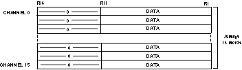
Without Zero or Zero-and-Overflow Suppression:
ECL port readout: EEN=1, ECE=0, OFS=X
CAMAC readout: CSR=1, CCE=0, OFS=X
DATA: 10-bit resolution: 0 to 1023; overflow=2047
11-bit resolution: 0 to 1919; overflow=2047.
Click here for diagram
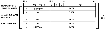
With Zero or Zero-and-Overflow Suppression:
ECL port readout: EEN=1, ECE=1, OFS=0 or 1
CAMAC readout: CSR=1, CCE=1, OFS=0 or 1
VSN: Virtual Station Number Loaded in the Status Register.
WC: Number of data words following the header word, 0 indicates 16 data words.
DATA: 10-bit resolution: 0 to 1023; overflow=2047 (only with OFS=0);
11-bit resolution: 0 to 1919; overflow=2047 (only with OFS=0);
SA: Channel Subaddress
Click here for diagram
CAMAC COMMANDS
Z: Initialize module; clear module and set status register's eight command bits to 1.
C: Clear the module.
I: Inhibit the front-panel gate when present.
X: Generated for all valid functions.
Q: Generated if a function can be executed.
L: LAM is set, if enabled, after the end of conversion (or ECL port readout) if
there are valid data to be read.
CAMAC FUNCTION CODES
F(0)ÀA(0): Read status word register. Q = 1 if BUSY = 0.
F(1)ÀA(0-15): Read pedestal memory (8 bits) for the 16 channels. Q = 1 if BUSY =
0.
F(2)ÀA(0-15): Random access or sequential readout of the 16 ADC values. Q = 1 if
BUSY = 1.
F(8)ÀA(0): Test LAM. Q = 1 if LAM is present.
F(9)ÀA(0): Clear module.
F(10)ÀA(0): Test and clear LAM.
F(16)ÀA(0): Write status word register. Q = 1 if BUSY = 0.
F(17)ÀA(0-15): Write pedestal memory (8 bits) for the 16 channels. Q = 1 if BUSY =
0.
F(25)ÀA(0): Enable test. Q = 1 if BUSY = 0.
CAMAC COMMANDS
X: Generated for all valid functions.
Q: Generated if a function can be executed.
CAMAC FUNCTION CODES
F(0)ÀA(0): Read DAC control register content (12 bits).
F(9)ÀA(0): Generates a clear signal on the COMMAND ECL bus.
F(16)ÀA(0): Write DAC control register content (12 bits).
CAMAC COMMANDS
Z: Reset memory address to zero and clear the LAM.
X: Generated for all valid functions.
Q: Generated if a function can be executed.
L: LAM is generated on overflow (OVF).
CAMAC FUNCTION CODES
F(0)ÀA(0): Reads 16-bit data at the current memory address, and increments the
address by one at S2. No Q response is generated when the address pointer exceeds the
memory capacity.
F(1)ÀA(0): Read memory address (16 bits). The presence of the two most significant
bits indicates an address overflow.
F(1)ÀA(1): Read the port enable register (2 bits).
R2 ­p; R3
0 ­p; 0 ­p; All ports disabled.
0 ­p; 1 ­p; CAMAC enabled.
1 ­p; 0 ­p; Reserved.
1 ­p; 1 ­p; ECL front panel enabled.
F(2)ÀA(0): Reads 16-bit data at the current memory address. Decrements the address
by one at S2. No Q response generated after word at address zero has been read.
F(8)ÀA(0): Test LAM. Q = 1 if LAM is present.
F(10)ÀA(0): Test and clear LAM.
F(16)ÀA(0): Write 16-bit data at the current address. Increments the address by
one at S2. No Q response is generated when the address pointer exceeds the memory
capacity.
F(17)ÀA(0): Write memory address (14 bits).
F(17)ÀA(1): Write the port enable register (see F(1)ÀA(1) table).
F(24)ÀA(0): Disables LAM.
F(26)ÀA(0): Enables LAM. LAM is generated on overflow.
Copyright® November 1995. LeCroy is a registered trademark of LeCroy Corporation. All rights reserved. Information in this publicaction supersedes all earlier