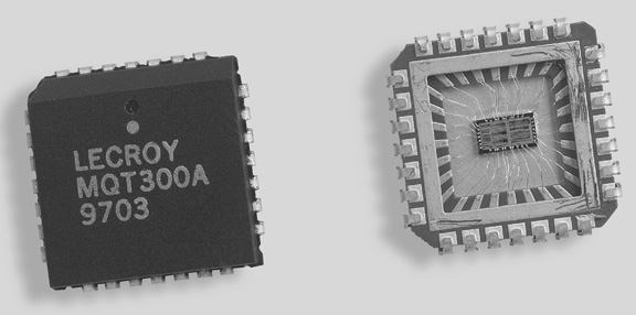
MQT300A CHARGE-TO-TIME CONVERTER |
|
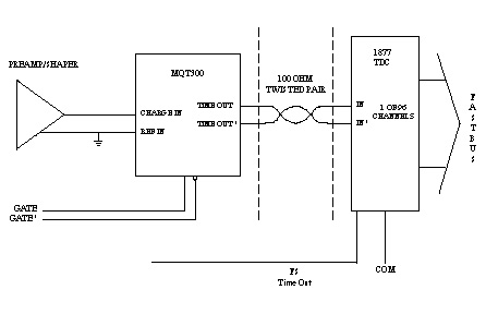
The LeCroy MQT300A is a wide range, high precision, monolithic charge-to-time converter. When combined with the LeCroy Model 1877S or 3377 Multihit, 500 psec TDCs, the MQT300A covers demanding ADC applications including fast plastic scintillators, BGO and CsI calorimeter readout. The wide dynamic range is achieved by overlapping three linear ranges having relative slopes of 1, 8 and 64. The outputs of the three converters are encoded into a single time stream so only a single channel of multihit TDC is required.
The MQT300A is ideal for high packaging density applications. Offering maximum flexibility with a minimum of support components, the high dynamic range MQT300A permits on-detector mounting near the preamplifier/shaper, away from the digital encoding, readout electronics and computer processing environment. Only balanced differential digital ECL signals are transmitted between the detector electronics and the readout electronics.
MQT300A OPERATION
This circuit handles the wide dynamic range of the input current by linearly splitting it into 3 integrator ranges with up to 50 mA of peak current. Maximum sensitivity is 50 fC/ps. Maximum full scale is 2620 pC above pedestal; Fast Clear time is 900 nsec, from the leading edge of the fast clear.
The MQT300A's single channel design minimizes crosstalk, optimizes Fast Clear response and simplifies board layout.
Figure 1: MQT300A and 1877 TDC Schematic
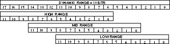
Figure 2: Dynamic Range Bit Alignment
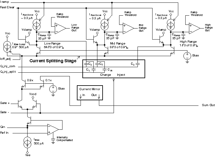
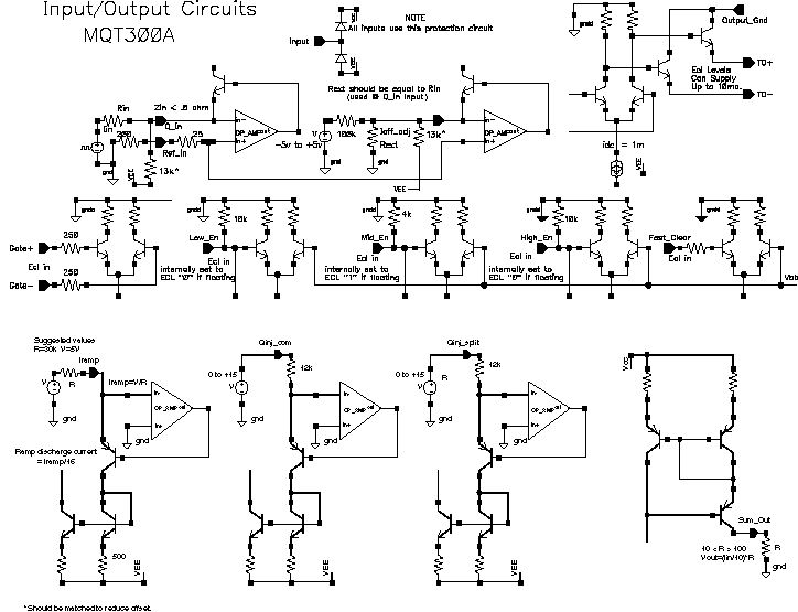
Figure 3 shows the basic elements of the front end. The input stage is formed by a
feedback stabilized common base transistor. The input current is received at the emitter
of the common base transistor. Low frequency common mode noise on the input signal and its
ground return can be rejected by connecting the input signal ground to the REF IN pin of
the MQT300A. The input current then goes through a gating differential pair. Ten percent
of the gated current is split off to the Sum Out current mirror which inverts the current
polarity and provides an output compliance range that includes ground. The remaining
ninety percent of the gated current goes into a current splitting stage. Here the gain of
the 3 ranges is determined. Each portion of the split current goes to a Wilkinson dual
slope converter. While the gate is open, charge is added to the integrating 35 pF
capacitor causing a voltage excursion directly proportional to the amount of input charge
on that range. After the gate closes a current (Iramp) is supplied to return the capacitor
to its quiescent level. The time it takes to restore the charge is directly proportional
to the amount of charge originally added. A comparator monitoring the ramp waveform on the
35 pF capacitor provides a digital pulse width corresponding to the input charge. The
comparator outputs can be individually disabled by ECL level control inputs.
Figure 3: The basic elements of the front end of the MQT300A
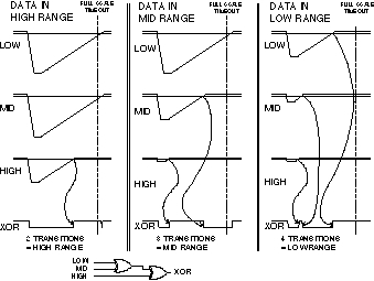
The operation of the three-range front end is shown in Figure 4 for three different input charge levels. The outputs of the three comparators go through an exclusive-or gate structure and produce a series of pulses which contain both the time data and the range identification.
Figure 4: Operation of the three range front-end
A large charge arriving at the front end causes the LOW and MID ranges to go to full scale. The data of interest is in the HIGH range whose ramp is above pedestal but below full scale. Two transitions would be recorded in a time-to-digital converter (TDC).
A medium range charge sends the LOW range to full scale. But both the MID and HIGH ranges are below the full scale time out. In this case the TDC sees three transitions and the data of interest is known to be in the MID range.
A small charge produces outputs from all three ranges. Four transitions are recorded in the TDC, indicating that the data of interest came from the LOW range. This case is similar to the pedestal condition.
When no charge is injected into the front end a pedestal condition exists. The pedestal is stable and predictable over both temperature variation and over gate width variation. The pedestals are set for approximately 700 nsec on the LOW range, 600 nsec on the MID range and 500 nsec on the HIGH range, with respect to the trailing edge of the gate.
This relatively large pedestal on the LOW range is provided by design to allow for uncompensated input offset currents which may be created in a DC-coupled configuration. Small offset errors in both the MQT300A's input and in the source of the signal will cause input charge. This charge can be of either polarity depending on the offsets. For example, a 3 mV negative input offset voltage in the MQT300A Q In can produce 15 µA into a 200 ohm input resistor tied to ground. With a 100 nsec gate this results in a 1.5 pC loss of pedestal charge and a reduction of pedestal by 150 nsec on the low range. The I OFF_ADJ pin can be used to trim out the error current. When this is done pedestal variation with changing gate width is minimized.
Two control pins provide direct adjustment of the pedestals. They are voltage sensing and may be connected to reference voltages or to DACs to provide system wide common pedestal adjustments. The Q_INJ_COM pin increases or decreases the pedestal of all these ranges by a similar amount. The Q_INJ_SPLIT pin injects a proportional amount of pedestal into the low and mid range with the greatest proportion going into the low range and the least proportion going into the mid range.
All ranges within their linear rundown range will complete within 5 µs (earlier with larger Iramp currents). This maximum time out can be selected by the user to trade off conversion time against resolution. At that maximum time the common start time out of the TDC (typically 1877S (or VT960)) should be applied by the user starting the conversion process. For faster conversion time, a fast clear pulse should be applied to restore all ranges (possibly saturated) to their quiescent state in parallel with the TDC conversion.
The VT960 and 1877S have a built-in auto ranging designed to operate specifically with the MQT300A. These units include a 2-bit field in the data stream indicating the number of edges recorded during the common start interval. The TDC is programmed to read out only the last edge received within the common start interval. The 2-bit field allows range identification of the data word providing an auto ranging feature. It is possible to readout the last 2 edges recorded which can be combined in a weighted average to minimize errors at range change overs and also to aid calibration between the ranges. It is also possible to read out all edges but this is normally only for debugging.
Three range enable bits are provided to allow flexible configuration of the MQT300A. When all three ranges are simultaneously enabled, the operation is as described above. Two range or one range operation is achieved by appropriate enabling of two or one ranges.
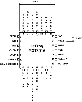
MQT300A IC PIN ASSIGNMENTS
PLCC 28
Pin 1: Sum Out: Current Output representing 10% of the gated input current. Inverting.
Pin 2: Vcca: +5 V
Pin 3: I OFF_ADJ: Input Offset Current adjustment input. Similar to Q In.
Pin 4: Vee: -5.2 V
Pin 5: Ref In: Analog Reference Input, high impedance ground reference.
Pin 6: Q In: Analog Charge Input, low impedance signal input.
Pin 7: Vee: -5.2V
Pin 8: Ground (Digital)
Pin 9: Vccd: +5 V
Pin 10: Vee: -5.2 V
Pin 11: Q_INJ_COM: Voltage supplied to this input increases pedestal for all 3 ranges by an equal amount. Nominal voltage is 7 V.
Pin 12: Low En: Low Range Enable, single-ended ECL levels.
Pin 13: Mid En: Mid Range Enable, single-ended ECL levels.
Pin 14: Q_INJ_SPLIT: Voltage supplied to this input supplies an increase in the pedestal of the low and mid range with the greatest proportion going to the low range. Nominal voltage is 7 V.
Pin 15: High En: High Range Enable, single-ended ECL level.
Pin 16: Fast Clear: Fast Clear input, single ended, ECL level.
Pin 17: TO -: Time Output, Differential ECL levels.
Pin 18: TO +: Time Output, Differential ECL levels.
Pin 19: Ground (Output)
Pin 20: Vclamp: +15 V
Pin 21: Ground (Digital)
Pin 22: Vee: -5.2 V
Pin 23: Ground (Analog)
Pin 24: Vcca: +5 V
Pin 25: Vcc: +15 V
Pin 26: Gate +: Differential Gate Input, ECL Levels
Pin 27: Gate -: Differential Gate Input, ECL Levels
Pin 28: IRAMP: Current supplied to this virtual ground input increases rundown current and decreases rundown time. Allows gain adjustment (320 µA for a gain of 50 ns/pC).
MIN |
NOM |
MAX |
Unit |
Comment | |
| DC Characteristics | |||||
| Vcc Voltage Requirement | 14.75 |
15 | 15.25 | V | |
| Vclamp Voltage Requirement | 14.5 | 15 | 15.5 | V | |
| Vcca Voltage Requirement | 4.75 | 5 | 5.25 | V | |
| Vccd Voltage Requirement | 4.75 | 5 | 5.25 | V | |
| Vee Voltage Requirement | 5 | -5.2 | -5.4 | V | |
| Vcc Current Requirement | 19 | 23 | mA | Static Condition | |
| Vclamp Current Requirement | 0.2 | 0.24 | mA | Static Condition (during pulse max. current can be up to 50 mA) | |
| Vcca Current Requirement | 22 | 27 | mA | Static Condition | |
| Vccd Current Requirement | 0.5 | 0.6 | mA | Static Condition (during pulse max. current can be up to 50 mA) | |
| Vee Current Requirement | 46 | 55 | mA | Static Condition | |
| Power Dissipation | 670 | 803 | mW | Static Condition | |
| Operating Range | |||||
| Temperature | 0 | 70 | °C | Case Temperautre | |
| Iramp (discharge current) | 320 | 1400 | µA | See Note 3 | |
| VQinj Com | 5 | 15 | V | ||
| VQinj Split | 5 | 15 | V | ||
| All characterization with 500 nsec gate width, Iramp=320 µA, VQinj Com=5, RIN=200 ohm, temperature=25°C, unless otherwise specified. | |||||
| Q In Characteristics | |||||
| Pulse Input Current Negative | 50 | mA | |||
| Input Current Positive | 0.2 | mA | |||
| Input Impedance | 0.15 | 0.5 | ohm | ||
| Rise Time | 3 | ns | For Specified Performance. | ||
| Common Mode Rejection | 60 | dB | DC to 100 kHz approx. = to 100 mV Common Mode Range | ||
| Series Input Resistor (Rin) (sets input impedance) |
100 | 200 | ohm | Larger value of R minimizes pedestal shift due to DC offset errors, for voltage source drive. Current source drive highly recommended. | |
| DC Input Signal Current | 10 | mA | |||
| Pulse Input Signal | 50 | mA | Pulse width must be < = 1 µs | ||
| Qin Error Voltage (V1) | -5 | 1 | mV | See Note 4 | |
| Ioffset ADJ Error Voltage (V2) | -2 | 2 | mV | See Note 4 | |
| Temp Coefficient of V1 | 28.5 | 100 | µV/°C | ||
| Temp Coefficient of V2 | 3.5 | 40 | µV/°C | ||
| Offset Current | |||||
|
-13 | 0.24 | 13 | µA | |
|
-50 | 6 | 50 | µA | |
|
-450 | 120 | 600 | µA | |
| Temperature Coefficient of Offset Curent | |||||
|
-0.03 | µA/°C | |||
|
-0.149 | µA/°C | |||
|
-0.299 | µA/°C | |||
| Gate Input Characteristics Differential ECL | |||||
| Duration | 10 | 500 | ns | Dynamic range and noise will be reduced for very small widths. Contact Factory for wider width options. | |
| Internal Settling Time | 5 | ns | |||
| Capacitance | 3 | 5 | pF | ||
| High Level | -0.9 | -0.8 | -0.7 | V | Integrate (Gate open) for Gate + Signal, Gate - signal requires opposite polarity |
| Low Level | -2 | -1.6 | -1.4 | V | Isolate (Gate closed) for Gate + Signal, Gate - signal requires opposite polarity |
| Rise/Fall time | 2 | 10 | ns | ||
| Pedestal Sensitivity to Temperature | |||||
| Includes effects of temperature coefficients of offset current. | |||||
| Lo Range, 50 ns Gate | -30 | 15 | 30 | fC/°C | |
| Mid Range, 50 ns Gate | -45 | 20 | 45 | fC/°C | |
| Hi Range, 50 ns Gate | -800 | 200 | 800 | fC/°C | |
| Lo Range, 1 µs Gate | -70 | 30 | 70 | fC/°C | RIN = 1K |
| Mid Range, 1 µs Gate | -340 | 50 | 340 | fC/°C | RIN = 1K |
| Hi Range, 1 µs Gate | -3500 | 1000 | 4500 | fC/°C | RIN = 1K |
| Pedestal Sensitivity to Vee (-5.4 to -5.0 V) | |||||
| Lo Range | -1.3 | 0.38 | 2.1 | fC/mV | See note 1 |
| Mid Range | -2.6 | 0.44 | 3.5 | fC/mV | See note 1 |
| Hi Range | -27 | 2.0 | 32 | fC/mV | |
| Pedestal Sensitivity to Vcca (4.75 to 5.25 V) | |||||
| Lo Range | -0.64 | -0.33 | 0.3 | fC/mV | |
| Mid Range | -2.5 | -1.44 | 1.0 | fC/mV | |
| Hi Range | -140 | 10.0 | 160 | fC/mV | |
| Pedestal Sensitivity to Vcc (14.75 to 15.25 V) | |||||
| Lo Range | -0.32 | -0.043 | 0.18 | fC/mV | |
| Mid Range | -0.50 | 0.057 | 0.65 | fC/mV | |
| Hi Range | -8.4 | 1.23 | 10.8 | fC/mV | |
| Gain Sensitivity to Temperature | |||||
| Lo Range | -0.01 | %/°C | |||
| Mid Range | -0.1 | %/°C | |||
| Hi Range | -0.1 | %/°C | |||
| Gain Sensitivity to Vee (-5.4 to -5 V) | |||||
| Lo Range | -0.5 | 0.57 | 2.0 | %/V | |
| Mid Range | -0.1 | 0.43 | 1.5 | %/V | |
| Hi Range | -0.5 | 0.54 | 2.0 | %/V | |
| Gain Sensitivity to Vcc (14.75 to 15.25 V) | |||||
| Lo Range | -0.72 | -0.16 | 0.58 | %/V | |
| Mid Range | -0.30 | -0.11 | 0.15 | %/V | |
| Hi Range | -0.42 | -0.20 | 0.12 | %/V | |
| Gain Sensitivity to Vcca (4.75 to 5.25 V) | |||||
| Lo Range | -0.5 | -0.094 | 0.39 | %/V | |
| Mid Range | -0.6 | -0.11 | 0.3 | %/V | |
| Hi Range | -1.5 | -0.20 | 0.8 | %/V | |
| Qinj Split Gain | |||||
| Lo Range | 0.68 | 0.86 | 1.0 | fC/mV | |
| Mid Range | 2.6 | 3.4 | 4.1 | fC/mV | |
| Qinj Com Gain | |||||
| Lo Range | 1.3 | 1.7 | 2.2 | fC/mV | |
| Mid Range | 11.6 | 14.6 | 17.5 | fC/mV | |
| Hi Range | 92 | 116 | 140 | fC/mV | |
| Time Output Characteristics | Differential ECL | ||||
| Rise/Fall times | 3 | ns | 20-80%, loaded with 510 ohm to Vee | ||
| High Level Voltage | -0.7 | -0.95 | V | ||
| Low Level Voltage | -1.85 | -1.5 | V | ||
| Output Current | 8.6 | 10 | mA | Recommended pulldown is 510 ohm to Vee | |
| Sum Output Characteristics | |||||
| Gain (Output Current/Input Current) | -0.09 | -0.1 | -0.11 | mA/mA | Inverting with respect to input current |
| Output Compliance | 0 | 5 | V | ||
| Offset Current | 3.8 | 7 | µA | ||
| Pedestal Charge | 300 | 800 | fC | Occurs immediately after leading edge of the gate | |
| Conversion Characteristics | |||||
| Mid Range Gain | 5.8 | 6.25 | 6.7 | ns/pC | See Note 2 |
| Lo Range/Mid Range Gain Ratio | 6.8 | 7.5 | 8.5 | ||
| Mid Range/Hi Range Gain Ratio | 7.0 | 8 | 8.9 | ||
| Full Scale Charge Beyond Pedestal | 2620 | pC | |||
| Residual Pedestal Low Range | 800 | ns | Input open or AC coupled, TG = 500 ns, QINJ_COM = 4 V, QINJ_SPLIT = 6 V | ||
| Residual Pedestal Mid Range | 650 | ns | Input open or AC coupled, TG = 500 ns, QINJ_COM = 4 V,QINJ_SPLIT = 6 V | ||
| Residual Pedestal High Range | 500 | ns | Input open or AC coupled, TG = 500 ns, QINJ_COM = 4 V, QINJ_SPLIT = 6 V | ||
| Fast Clear | |||||
| Pulse Width | 300 | ns | |||
| Settling Time (after pulse) | 600 |
ns | To settle to within 0.1% with Iramp=320 µA | ||
| Integral Non-linearity | |||||
| Lo Range | ±0.03% of full scale | ±0.15% | 200 ohm input, TG = 50 ns sampled mode | ||
| Mid Range | ±0.05% of full scale | ±0.3% | 200 ohm input, TG = 50 ns sampled mode | ||
| Hi Range | ±0.02% of full scale | 200 ohm input, TG = 50 ns sampled mode | |||
| Composite of all 3 Ranges (algorithm dependent) | ±0.3% of input +20 fC | 200 ohm input, TG = 50 ns sampled mode | |||
| Noise Charge Qnoise = k1 (square root of) Tg+k2x10-9) pC (rms) | |||||
| Lo Range Hi Z Input | |||||
|
25 | 50 |
|||
|
180 | ||||
|
12x10-3 | pC (rms) | |||
| Lo Range 200 ohm Input | |||||
|
39 | 80 | |||
|
100 | ||||
|
15x10-3 | pC (rms) | |||
| Mid Range | |||||
|
208 | 420 |
|||
|
180 | ||||
|
0.1 | pC (rms) | |||
| Hi Range | |||||
|
1350 | 2700 | |||
|
300 | ||||
|
0.8 | pC (rms) | |||
| where Tg=gate width (in seconds) | |||||
Note 1
Vee sensitivity can be improved for these ranges by returning the two 13k bias current resistors on Qin and I_Off_Adj (see Input/Output Circuits schematic) to a reference supply (instead of Vee).
Note 2
The maximum sensitivity of 50 ns/pC (for the Lo Range) is obtained with Iramp set to 320 µA. This current is internal divided by a factor of approximately 16 which yields a final ramp run-up current of 20 µA. The maximum sensitivity of 50 ns/pC is equivalent to 20 fC/ns.
Note 3
Iramp is set by selecting the value of R and V (see Input/Output Circuits) Iramp =V/R. This current is internally divided by approxi-mately 16, mirrored and supplied to the ramp as discharge current to set the ramp back to its quiescent level. The time for the ramp to recover to this level is equivalent to the output time. For a gain of 50 ns/pC low range, (6.25 ns/pC mid range, 0.78 ns/pC hi range) the required discharge current would be equal to 20 µA. (I=Q/t).
Note 4
The input stage requires a fixed operating current (Ix) to maintain linearity; this
current added to the input current is applied to the Ramp Cap. To prevent a large pedestal
from occurring, a compensation current (Icomp) must be generated, and subtracted from Ix.
Ideally Ix and Icomp are equal, but due to process and thermal variants, the two currents
may not be exactly equal. The difference between them is referred to as the Offset
Current. Ix and Icomp are generated externally by the 13K resistors (refer to Input/Output
Circuits) these resistors should therefore be matched (1% or better) to reduce the Offset
Current. V1 is defined as the voltage between Qin and Ref In. Ideally this voltage would
be equal to zero, but due to a finite open loop gain of the input feedback amplifier, it
is close to, but not equal to zero. This voltage plus any offset voltage due to the
source, divided by Rin plus the Source Resistance (Rsource) produces a component of the
offset current. To compensate for this component Rext is connected from Ioff_ adj to
ground. Rext should be equal to Rin plus Rsource. V2 is the voltage between Ioffset_adj
and Qin, similar to V1 it also has an offset associated with it. The resulting external
component of offset current can be expressed by
Ioffset=Ix-Icomp+(V1+Voffset)/(Rin+Rsource)-V2/Rext. If the MQT300A is driven from a
current source (Rin approaches infinity, and also Rext since Rext should be equal to Rin)
a major portion of the external component of offset current is eliminated. For wide Gate
Widths current source drive is recommended.
Figure 5: Input/Output Circuits MQT300A
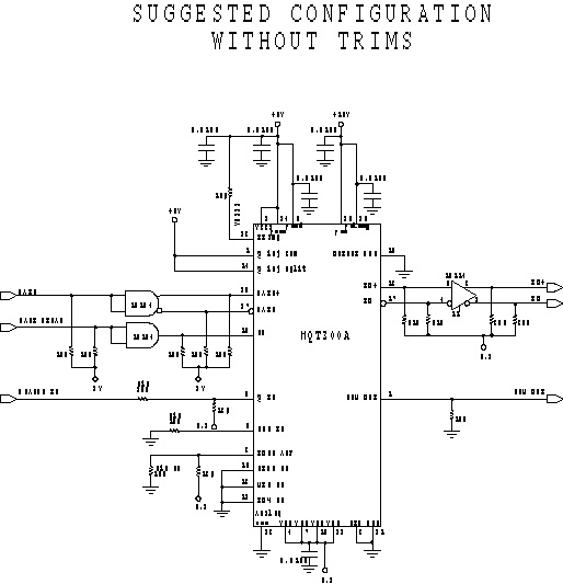
Figure 6: Suggested Configuration Without Trims
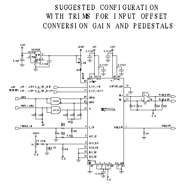
Figure 7: Suggested Configuration With Trims for Input Offset Conversion Gain and Pedestal
Figure 8: MQT300A Pin Assignments
Copyright© September 1997. LeCroy is a registered trademark of LeCroy Corporation. All rights reserved. Information in this publication supersedes all earlier versions.