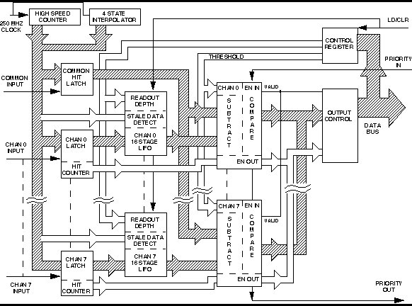
The MTD133B integrated circuit is a full custom CMOS circuit which measures the separation in time between transitions (hits) arriving at the COMMON input and each of eight independent channel inputs. Each channel accepts up to 16 hits. Time differences are measured with 500 psec least count. The MTD133B is packaged in a 68-pin PLCC.
The MTD135 is a modification of the MTD133B. The only change visible to the user is the signal input. The inputs have been changed from differential PECL to single ended CMOS, to reduce the power dissipation. The functional behavior, most specifi cations, the package and the pinout (with the exception of the inputs) are identical to the MTD133B. The inputs are inverted with respect to the MTD133B, a logic 0 to 1 transition (0 to 5 V) on the input will be recorded as a negative edge, the same as a 1 to 0 transition on the PECL input of the MTD133B. The only other change is to the internal structure of the MTD135. The LIFO memory storage has been modified to eliminate the high current surge on power up.
The MTD133B measures time intervals by recording the arrival time of edges on its inputs. These times are then subtracted from the arrival time of a Common input. Storage for 16 hits per channel is provided. Circuitry is included to limit the full scale time, remove ambiguities due to roll over of the counter, limit the number of hits per channel, and maximize readout speeds.
The Time Base consists of a 16-bit counter and a delay line interpolator. The interpolator extends the time measurement with two additional LSBs for an 18-bit full scale. The 16-bit counter counts at twice the frequency of the external acquisition clock (ACLK). Thus, with a 250 MHz external clock, the counter moves at 500 MHz, its LSB measuring 2 nsec intervals. The delay line interpolator divides this interval into 4, 0.5 nsec intervals.
The 16-bit counter uses a gray code rather than binary. This limits the number of changing bits with each clock edge to one. When this code is latched while a bit is changing, the value recorded in the latch is one of two consecutive codes. In binary, numerous bits may change on each clock edge and if one is latched incorrectly, the error could be large.
The interpolator has three output bits. Between the 16-bit counter state changes, each of these outputs change state once. While the output is not the standard gray code, it does have the property of only one output changing at a time.
All nineteen bits of the Time Base are bused to the Hit Latch of each channel and a Common Hit Latch. When an edge arrives, which the MTD133B is programmed to record, the current value of the Time base is recorded in the Hit Latch. The Common Hit Latch records data based on the Common Hit (COM) input only.
Each channel has a LIFO storage element. This LIFO accepts hits as long as the chip is write enabled (WE). When the number of data word exceeds the depth of the LIFO the oldest data word, the first stored, is lost. The LIFO has a maximum depth of 16 and can be programmed to any depth between 1 and 16.
To maintain the status of data words in the LIFO, a status bit, VALID, is included with each data word. When data enters the LIFO, VALID is set to one. When, for any reason, the data word is to be purged from the LIFO, VALID is cleared. A data reset (LD/CLR) clears all these status bits. The data remains but is inaccessible. The programmable depth of the LIFO is effected by clearing status bits of data words which move beyond the programmed depth. As data words are shifted out of the LIFO, empty locations are indicated with VALID equal to zero.
While data is stored in the LIFO, it is possible for the counter in the Time Base to roll over. If this occurred the computation (subtraction) of a time interval would be incorrect by a full scale time. This problem is avoided, in part, by the Stale Data detection algorithm.
Internally, the MTD133B works with an 18-bit dynamic range. The additional bits added to the counter allow data which is more than a 16-bit range away from the current value of the counter to be invalidated. Since only the three MSBs are used, this algorithm is coarse in that it will pass data which should be invalid. But, it does not pass any data that is ambiguous in the 18-bit subtraction, done during the readout phase.
During acquisition, arrival times are stored. During readout, the data is processed to compute time intervals. Before readout begins, three readout clocks (priming clocks) are required to fill the readout pipeline.
The first pipeline stage converts the 19-bit time value to an 18-bit binary format. This conversion is a standard Gray to binary for the 16 most significant digits. The remaining 3 interpolator bits are priority encoded. An entire stage in the pipeline is given to this conversion because a carry must propagate from the MSB to the LSB.
The second stage of the pipeline performs the subtraction from the Common Hit. The sense of the subtraction depends on the mode used (i.e. Common Start or Common Stop). The carry for any subtraction propagates from the LSB to MSB. If either of the two MSBs are non-zero, the data is marked invalid.
Within this same pipeline stage, the result of the subtraction is compared to a threshold. If the data exceeds this threshold it is also marked as invalid.
The comparison is possible in this pipeline stage because the carry for the comparison propagates in the same direction as the previous subtraction. This causes the additional time required by the comparison to be minimal.
The third stage of the readout pipeline is used to select the next channel to be driven to the external bus. While data is being asserted on the output bus, valid data bits are being checked to find the next data word to be output. If the remainder of the chip is empty, the Priority Out (POUT*) is asserted, passing future control of the output bus to another chip. The chip asserting Priority Out tri-states the output bus on the next readout clock.
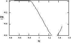
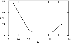
The MTD133B interpolator consists of an adjustable delay line composed of four delay elements. The Acquisition Clock (ACLK) enters this delay line to generate five versions of ACLK, P0, P1, P2, P3, and P4. P0 has no delay, but is synchro nized with transition of the coarse counter, and P4 is delayed by four delay elements. To achieve correct operation the delay line must be adjusted such that P4 is exactly 180� out of phase with P0.
To monitor the state of the delay line, two phase comparators are included. The first, DN, implements the logic equation "P0 and P4 and not P2". This equation becomes true for a brief period if P0 and P4 are not 180� out of phase because the delays are too long ("not P2" is only useful when the delay are very far from correct). Further, the time this equation is true is proportional to the error in delay. The pin DN sinks current to ground while the equation is true.
The plots in Figures 1 and 2 show current (mA) at the DN as a function of the approximate delay (nsec) of a single delay element. The acquisition clock is at 150 MHz and requires 833 psec delay to operate correctly. When the delay (controlled by DCN and DCP) exceeds 833 ps, DN begins to sink current.
The MTD133B current usage varies with its activity. On initial power up the current can go as high as 400 mA and then falls slowly. This condition will persist until the MTD133B receives hits, either by inputs or the internal tester. After receiving hits, the MTD133B will draw 60 to 90 mA, depending on the Acquisition clock frequency. With a 250 MHz Acquisition clock the MTD draws 90 mA typically.
Figure 1: The pin DP implements a complementary phase comparator which sources current when the delays are too short.
Figure 2: This arrangement of sink and sourcing current is intended to allow the DN and DP pins to be wired together. The combination is used to control the speed of the interpolator via DCN and DCP.
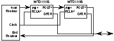
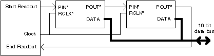
Figure 3: Typical connections for multi-chip readout.
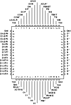
MTD133B Pin Descriptions and Pin Out Diagram.
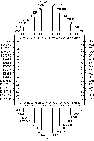
MTD135 Pin Descriptions and Pin Out Diagram.
The Acquisition Clock uses differential positive ECL levels. This clock sets the fundamental time base for the MTD133B, and drives a gray code counter. This counter runs at twice the clock frequency by incrementing on both edges of the clock. Further, the Interpolator section creates three delayed versions of the Acquisition clock, dividing each 1/2 clock period into four parts. Thus, the time base of the MTD133B counts at eight times the Acquisition Clock. If the Acquisition Clock is set to 250 MHz, the Least Significant Bit of a time measurement represents 500 ps. Because of the way the Acquisition Clock is used, the duty cycle directly contributes to the differential non-linearity and should be as close to fifty percent as possible. The 60/40 duty cycle of typical crystal oscillators is not adequate.
The Common Hit input uses differential Positive ECL (PECL) levels. The arrival time of a positive edge (rising) to this input is recorded in the Common Hit Register. During readout, the data from channel inputs is subtracted from the Common Hit Register (Common Stop Mode) or the Common Hit Register is subtracted from the channel data (Common Start Mode), to compute the time interval. Multiple positive transitions, during acquisition time, on the Common Hit input are acceptable. Only the last transition has any effect on the final data. The common hit must return to the false state before the start of readout.
The MTD133B Channel Inputs use differential Positive ECL (PECL) levels. These inputs are also compatible with CMOS inputs where the complementary inputs are driven to the threshold voltage. The arrival time of both positive and negative transitions on the Channel inputs may be recorded, according to configuration pins PE and NE. The recorded data is put in the LIFO for later comparison to the Common Hit.
Write Enable is an active high CMOS input. Data is acquired by the channel inputs and test input only while Write Enable is asserted. Write Enable does not control the Common Hit input; common hits must be prevented by external logic for correct operation.
Test is a CMOS input. When both Write Enable (WE) and Test Enable (TE) are asserted, transitions on Test are copied to all eight channel inputs. The Test input bypasses the differential ECL receiver, all other structures are tested, including double pulse protection circuits.
Test Enable is an active high CMOS input. When asserted, in combination with Write Enable, the Test input is enabled and the Channel inputs are disabled.
Mode is a CMOS input. When low, the MTD133B works in Common Stop mode, otherwise Common Start mode.
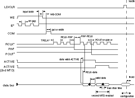
LD/CLR is an active high CMOS input. LD/CLR is used to latch register data into the MTD133B. When the MTD133B Data Bus is tri-state, it is driven from an external source and a falling edge on LD/CLR latches the data into the Threshold and Depth registers. LD/CLR also clears all data from the memory and readout pipeline. The Common hit register is set to zero. An LD/CLR pulse should be applied during initialization and after EVERY readout.
Positive Edge Enable and Negative Edge Enable are active high CMOS inputs. The Positive (Negative) Edge enable allows rising (falling) edges to be recorded and stored in the LIFO storage structure. PE and NE may be asserted in any combination. Deasserting both results in no data being recorded.
When used with LD/CLR, the binary data value on these pins set the depth of the LIFO storage. Any data pushed beyond the specified depth is lost. A value of zero indicates a depth of 16 data words.
When used with LD/CLR, the binary data value on these pins sets the full scale, in counts, of the MTD133B. The four missing least significant bits (T3-T0) are treated as if they were set. In other words if T15 through T4 are set to zero, data values between zero and 15 are accepted. Time values greater than the value loaded are discarded.
Delay Control Negative and Delay Control Positive are analog current inputs. These inputs control the speed of the Interpolator. The Delay Control Negative (Positive) current is used to create the supply current for N-type (P-type) devices in the Interpolator delay line. The smaller the current, the slower the positive (negative) clock edges propagate through the Interpolator. The Delay Control Positive has an additional current mirror which makes the nominal current to ground the same for both inputs. They may be connected together to simplify the control of the Interpolator.
Delay Negative and Delay Positive are analog current outputs which monitor the speed of the Interpolator. Delay Negative connects to ground when clock edges are propagating through the Interpolator too quickly. Delay Positive connects to Vdd when clock edges are propagating though the Interpolator too slowly . The connect times, and consequently the currents are proportional to the error. The connect times occur at different phase of the Acquisition Clock. These outputs may be connected and through a single inverting stage, used to control DCN and DCP.
ROSC is a CMOS output of the Ring Oscillator. ROE (Ring Oscillator Enable) is an active high CMOS input. The Ring Oscillator is only used to estimate the speed of the process used to manufacture the MTD133B. The Ring Oscillator is constructed of 31 elements. In normal operation ROE is grounded.
Reset is an active high CMOS input. When Reset is asserted, the Gray counter in the time base is cleared. The counter begins to count correctly 16 Acquisition clocks after RESET is deasserted.
PIN* (Priority In) is an active low CMOS input. POUT* (Priority Out) is an active low CMOS output. When Priority In is asserted, the MTD133B drives the Data Bus (D15-D0, C2-C0, H0, H1, & PHASE) on the next RCLK* (falling edge) if data is available. New data is driven for each RCLK*. If data is not available for the next RCLK*, POUT* (Priority Out) is asserted immediately and the Data Bus is tri-stated on the next RCLK*. POUT* may be connected to PIN* of a different chip to form a readout chain. The propagation of Priority from one chip to the next allows new data to be asserted on every RCLK*, provided the chain is not too long or the presence of data can be guaranteed. The assertion of POUT* by the last device in the readout chain indicates that the last data word is being asserted and the Data Bus will tri-state on the next RCLK*.
Active is an active high CMOS output. When asserted it indicates that the device is asserting data on the Data Bus. Active changes state on the falling edge of RCLK*.
RCLK* (Readout Clock) is an active low CMOS input. The falling edge of this clock causes new data to be asserted on the Data Bus, if the data is ready and the device is enabled (PIN*). After the end of Acquisition (WE deasserted) not less than three priming clocks are required to fill the Readout Pipeline. After the first device in the readout chain is enabled, a new data word is asserted on each RCLK*. One additional RCLK* is required to tri-state the Data Bus (or RESET).
C2-C0 are active high CMOS outputs. These signals are part of the Data Bus and indicate which channel within the device the data originated from.
H0 and H1 are active high CMOS output. These signals are part of the Data Bus and indicate the number of hits (modulo 4) recorded in the current channel. This data is repeatedly asserted for each data word in the channel. This data is used in a multi-ranging ADC design.
Phase is an active high CMOS output. Phase is part of the Data Bus and indicates the type of edge recorded. High indicates a positive edge was recorded.
D15-D0 are active high CMOS bidirectional signals. During Readout, D15-D0 represent the
time measurements. When disabled, they may be driven in combination with LD/CLR to set the
Threshold and Depth registers. The Threshold register uses D15-D4 and the Depth register
uses D3-D0.
MODE, PE, and NE must be set to their appropriate DC levels prior to input. The Threshold and Depth registers are loaded via the data lines when the data lines are tri-state. Driving signal LD/CLR high resets the data in the MTD133B. Driving signal LD/CLR low latches the input as shown in the timing diagram in Figure 4. Driving LD/CLR high also clears all data from memory and the readout pipeline. This must be done for initialization and after each readout.
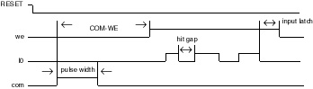
Figure 4: Common Stop and Data Output Timing Parameters.
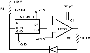
The following circuit can be used in a system which has a 250 MHz acquisition clock. It is similar to those used in the 1877 TDCs. These resistor values have been shown to work with an acquisition clock frequencies at 250 MHz. DCP and DCN are current inputs which control the delay in the Interpolator, (see DCP/DCN pin and Interpolator Control descriptions in this document). Vcc and R1 set the minimum current input to DCP and DCN. If a slower acquisition clock than 250 MHz is used, then R1 may need to be replaced by a larger value. The minimum current should be set to approximately half the amount needed for correct Interpolator delay. The resistor value needed can be determined experimentally by changing the value of R1, while the MTD133B is running at the desired Acquisition clock rate, until the amount of current flowing through R1 is approximately equal to that which flows through R2.
After all of the configuration DC inputs have been set and the MTD133B has recovered from reset the WE pin is asserted. While the WE pin is high the MTD133B will accept data on its input pins. The Common can be given either at the beginning or the end of the acquisition period, depending on the chip being run in Common Start or Common Stop mode. It is recommended that the common is given while the WE is low, either before or after the acquisition time to prevent the occurrence of negative events. In common stop mode this can be done by triggering the WE with the common and then delaying the common to the MTD133B.
After the acquisition period is over the MTD133B needs three priming clocks (RCLK*) to fill the Readout pipeline. MTD133B readout is initiated by PIN* going low. This must occur within a window during which RCLK* is low. After the first rising edge of RCLK* the MTD133B drives the active pin high and begins readout. The MTD133B then asserts data on the bus on each falling clock edge until the chip has completely read out its data. After the last data word has been asserted. POUT* is driven low and active is driven high. POUT* must occur while RCLK* is low and the designer must choose the frequency of RCLK* to ensure this. There is also some delay in the propagation of the Priority through a chip which contains no data, which must also be considered in determining the Readout Clock frequency. The data bus is tri-stated on the next RCLK* following POUT* and the next MTD133B will begin its readout. The timing diagrams in Figure 5 illustrate the acquisition and readout processes with Acquisition and Readout Clocks at 250 MHz and 10 MHz respectively.
Figure 5: Interpolator control circuit.
Most of the data in Table 1 was obtained by measuring the signals at the MTD133B in a 3377 CAMAC TDC, which utilizes a 250 MHz clock. Measurements were taken using 2 FET probes and a LeCroy 9324 scope. Some of these timing parameters are controlled by the design of the 3377 and are proven to work reliably. Minimum and maximum values of chip dependent parameters are not specified.
| Parameter Name | Value |
Comments |
| twidth | 50 ns | |
| thold | 10 ns | |
| input latch | 102 ns | Used in 3377 design |
| WE-COM | > 1 ns | Used in 3377 design prevents negative event times |
| hit gap | 10 ns | typical from design, guaranteed < 20 ns |
| pulse width | > 100 ns | Used in 3377 design |
| TRCLK | 100 ns | Period of Readout clock used in 3377 design |
| TRCLK | 50 ns | Period of Readout used in 1077 designs |
| RCLK-PIN* | 100 ns | Used in 3377 design |
| PIN*-RCLK | 145 ns | Used in 3377 design |
| POUT response | 22 ns | typical measured on sample chips in 3377 |
| RCLK-data | 12 ns | typical: measured on sample chips in 3377 |
| data valid-ACTIVE | 3 ns | typical: measured on sample chips in 3377 |
| transition time | 10 ns | typical: measured on sample chips in 3377 |
| valid data | 90 ns | Dependant on transition time and RCLK* rate |
| PIN*-POUT* (no data) | 3.5 ns | typical: measured on sample chips in 3377 (not on diagram) |
| Parameter Name | Value | Comments |
| COM-WE | >1 ns | Used in 3377 design, prevents negative hits |
| Minimum hit gap | 10 ns | Estimated from design |
| Common pulse width | > 100 ns | Used in 3377 design |
| Input latch | 102 ns | Used in 3377 design |
Internal test support allows makes it possible to simultaneously test all of the MTD133B inputs at once. The acquisition phase is the same as normal acquisition, except that the Test Enable (TE) pin configured high and the Test pin is pulsed to cause each hit while Write Enable (WE) is high. The channel inputs are disabled when the Test Enable is true.
Figure 6: Common Start Timing Parameters.
Figure 7: Typical connections for multi-chip readout.
Copyright� March 1998. LeCroy is a registered trademark of LeCroy Corporation. All rights reserved. Information in this publication supersedes all earlier versions.