|
|
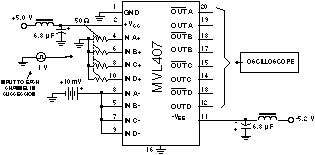
The Model MVL407 and the Model MVL407S are quad voltage comparators designed for
applications requiring ultra-high speed and accurate timing. The devices are manufactured
using a high speed bipolar process which results in an extremely short (3.5 nsec)
propagation delay with operation at speeds in excess of 400 MHz. The comparators are
available in two types of package; a standard 20-pin DIP (MVL407), or a surface-mount
version in a SOIC (Small Outline IC) package (MVL407S). Unpackaged die are also available
(MVL407D).
The MVL407 incorporates a unique hysteresis feature for exceptionally clean operation.
When the comparator changes state, an internal differential input offset of about 4.8 mV
is generated. This positive feedback drives the device quickly through its switching
region, greatly reducing the possibility of oscillation or output chatter with small or
slowly changing inputs. The propagation delay is typically 3.5 nsec and changes by only
100 psec across a 5 to 100 mV overdrive range. This very low delay variation makes these
comparators extremely useful in critical timing applications.
Each channel provides differential inputs and complementary outputs compatible with the
ECL logic family. The outputs can drive 50 W loads or 100 W twisted pair. (External
pull-down resistors are required.)
For evaluation and prototyping, the Model MVL407PK is recommended. It consists of a single
MVL407 mounted on a printed circuit board. Space is provided for user prototyping
circuitry. The power and reference voltage must be supplied to the board via a wire
pigtail.
SPECIFICATIONS TABLE
Interconnection Techniques
To achieve optimum performance, high speed circuits require some special layout
precautions. For a good low inductance ground current return path, a ground plane must be
used. The input impedance should be as low as is practical and lead lengths should be as
short as possible. The MVL407 should be soldered into the printed circuit board instead of
using a socket. To minimize ringing, output lead lengths of 2 cm or less are recommended.
If longer lengths are required, use a microstrip transmission line, miniature coaxial
cable, or twisted pair. Reflections will occur unless the line is properly termi nated.
Termination resistors typically go to -2.0 V. Low impedance lines are better for driving
capacitive loads. Supply voltages should be well decoupled with good RF capacitors
connected to the ground plane as close to the MVL407 supply pins as practical.
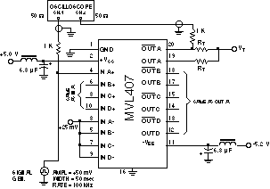
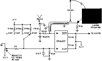
Propagation Delay Measurement
The ability of a voltage comparator to perform an accurate timing function is determined
by the constancy of its propagation delay with overdrive. Because the input rise time and
the comparator's slew time add in quadrature to produce the observed propagation delay, it
is necessary to employ a very fast input pulse to accurately measure propagation delay
variances of the device. A slow input would give optimistically low results. See Figures
8, 9, & 14.
In order to produce a sufficiently fast and clean input pulse, a tunnel diode based pulse
generator was employed. It produced a very clean pulse with a rise time (10% to 90%) of
approximately 0.1 nsec. See Figures 7 and 17.
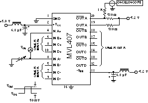
Double Pulse Resolution Measurement
To measure the double pulse resolution (DPR), the input pulse width was adjusted to the
minimum, which provides a full amplitude output. The delay of the second pulse was reduced
until a degradation of output amplitude was noted. The closest spacing of the input pulse
pair which will produce a second pulse of full output amplitude is considered to be the
DPR (Figure 5).
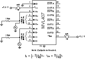
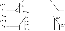
Hysteresis
The MVL407 incorporates about 4.8 mV of internal hysteresis, and therefore has two
thresholds separated by about 4.8 mV. One threshold (VT+) applies for input signals that
cause a low-to-high transition on the normally low output (e.g., a positive -going signal
applied to the IN+ output, or a negative-going signal applied to the IN - input). The
other (VT­p;) applies for input signals that cause a high-to-low transition on the
normally low output. The hysteresis voltage (V H) is the difference between these two
thresholds. V T+, VT­p; and VH are measured as shown in Figure 4.
The presence of this hysteresis helps assure that the outputs of the MVL407 are always in
a defined state, even for small or very slowly changing inputs. Comparators without
hysteresis show a pronounced tendency to oscillate when biased near threshold. In spite of
its higher speed, the MVL407 gives much cleaner operation than other comparators.
Figure 1
Figure 2
Figure 3
Figure 3B
Figure 4
Figure 5
Figure 6
Figure 7
Figure 8:
Propagation Delay as a Function of OverdriveFigure 15:
Response to 100 MHz sine wave.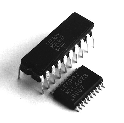