The Model TRA402 and the Model TRA402S are monolithic four-channel, fast,
low-noise amplifiers. The amplifiers are available in two types of packages,
a standard 22-pin DIP (TRA402), and a surface-mount version in a SOIC (Small
Outline IC) package (TRA402S). Their principle application is amplification
of wire chamber signals for time-resolved measurements. Their high density
make it a practical solution, especially if space at the detector is at
a premium, yet chamber mounting is a necessity.
The TRA402 has complementary inputs on all four channels. This feature allows
use of the amplifier with both positive and negative inputs provided by
the cathodes and anodes of a wire chamber respectively.
The amplifiers produce a gain of 25 mV/µA with a rise time of 3 nsec.
The low input impedance of < 100 ohm and low noise of < 100 nA R.M.S.
is ideally suited to chamber applications, providing little integration
of the current pulses. The special input geometry of the chip makes it useful
even with high capacitance detectors such as liquid argon calorimeters or
wire chamber strips and pads. Because the rise time of the wire input is
maintained by the TRA402, the user has greater freedom in selecting the
RC-coupling to the subsequent circuitry, allowing the rise time/noise trade-off
to be optimized.
The TRA402 is a high gain, high bandwidth device. Thus, good high frequency printed circuit layout techniques are required. Supply voltages must be properly decoupled and input and output trace routings must be well separated and kept to minimum lengths. Lead inductance is a potential feedback mechanism which can cause oscillations. One common cause of this effect is introduced by conventional IC sockets. These may not be used with the TRA402. Either insertion pins such as Berg Minisert pins (75060-12), or direct soldering into the board is a necessity. Only with attention to these matters can stable operation with minimum interchannel crosstalk be achieved. For most applications, a small inductor (bead) such as a Ferroxcube 56-590-65/4B (LeCroy 300-010 -001) or a 10 ohm resistor should be used in series with the output ground. See Figure 1.
Two supply voltages are required by the TRA402. By virtue of the design
of the amplifier, the voltage range listed must be observed to achieve the
electrical characteristics intrinsic to the device. In order to minimize
the possibil ity of oscillation, the positive supply voltage for the amplifier
(Pins 11 and 22) and the output emitter follower (Pin 14) are separate pins.
Bypassing both supplies should be as shown in Figure 1. Capacitors with
good high frequency characteristics must be used. Capacitors of at least
.01 µF are recommended.
The bandwidth, output swing, conversion gain and noise performance of the
TRA402 are affected by the supply voltages. See Figures 5-8. In general,
lower supply voltages give better noise performance at the expense of output
swing, gain and response time. The optimum performance must be selected
on a case by case basis.
The front end of the TRA402 is a differential current amplifier. Both
inputs are biased to approximately -0.7 V. Thus, any DC path to ground resulting
in an input current, must be avoided. Unless an extremely high impedance
source (e.g., a proportional chamber wire) is employed, the inputs must
be capacitively coupled.
Each input of the chip consists of a common base stage with the base connected
to DC ground. The emitter standing current (0.34 mA) at each input is supplied
by an internal current source. This configuration results in a typical input
impedance of 85 ohm.
All inputs are protected against low level positive over-voltage transients
with internally connected small junction area protection diodes to ground.
For low level negative over-voltage, the emitter to base diode of the input
transistor acts as a protection diode. To protect the inputs against large
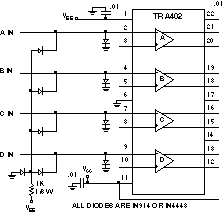
transients, two diodes should be installed at the input. Use a fast, high
conductance diode such as 1N914 or 1N4448. See Figure 3.
Since the quiescent output level is not 0.0 V, it is recommended that
the outputs be capacitively coupled, as shown in Figures 1 and 9. An output
network that serves as DC blocking may also be used to achieve RC shap ing.
If the amplifier and its load are to be separated, pickup and noise considerations
recommend that the shaping be located at the load. The output can drive
50 ohm, making it suitable for use with coax cable. With the TRA402, driving
a low impedance load, the amplitude is attenuated due to its non-zero output
impedance. Noise, crosstalk and pickup set an upper limit on the length
of cable that can be driven. For long cable runs, shielded twisted-pair
cable is recommended.
The maximum positive voltage swing of the TRA402 is typically >1 V across
50 ohm and is sufficiently high in most applications. The maximum negative
output voltage swing, however, is much smaller and given by the DC standing
current in the output emitter followers of the device. The standing current
is typically 1.4 mA. This current allows driving a 50 ohm load with a maximum
negative voltage swing of 1.4 mA · 50 ohm = 70 mV. In cases where
this voltage swing is too small, the user may increase the DC standing current
in the output emitter fol lower. This is accomplished by adding an external
pull-down resistor per output to a negative voltage. The nega tive voltage
to which the pull-down resistors are connected can be either V EE or a separate,
more negative voltage than VEE which results in somewhat better linearity.
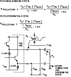
The value for the pull-down resistors can be calculated by the formulas
given in Figure 9. These formulas allow for a residual DC standing current
of 0.4 mA in the output emitter follower for good linearity.
The output of each TRA402 channel is a differential driver. For single-ended
applications, the used and unused outputs should be terminated symmetrically
for stable operation.
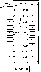
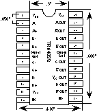
Model TRA402 and TRA402S
Pin Assignments. Alternate packaging including LCC are available.
Figure 1: Test Circuit for TRA402 Evaluation
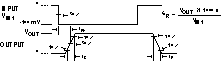
Figure 2: Definition and measurement of gain propagation
delay and output signal rise and fall times.
Figure 3: Suggested Input Protection
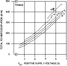
Figure 4: Power dissipation versus VCC and for
V EE between -2 V and -3.5 V. The data were taken with no external pull-down
resistors.
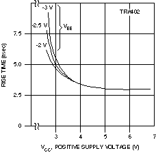
Figure 5: Output signal rise time versus VCC for
three different values of V EE with the outputs terminated into 50 ohm.
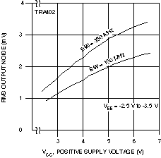
Figure 6: R.M.S. output voltage noise vs. VCC.
V EE is not critical and can be set anywhere between -2.5 V and -3.5 V.
The upper trace shows the noise when measured with a 350 MHz bandwidth,
the lower trace was taken with 100 MHz bandwidth.
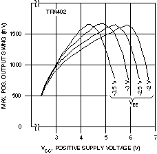
Figure 7: Maximum positive output voltage swing
(into a 50 ohm load) of TRA402 versus V CC. The graph shows signal swing
for various values of V EE.
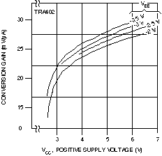
Figure 8: Conversion Gain versus VCC for values
of V EE between -2 V and -3.5 V. Data were taken with outputs terminated
into 50 ohm.
Figure 9: The formulas shown in Figure 9 are used
to calculate the pull-down resistors for a desired negative going output
voltage swing.
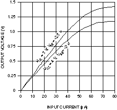
Figure 10: Linearity plot for the TRA402 using
a current pulse as input signal. The plot shows the positive output signal
only. Similar results are achieved with charge pulses as input signal.
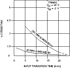
Figure 11: Channel-to-channel crosstalk measured
on the TRA402 plotted as the peak output voltage in any inactive channel
divided by the peak output voltage of the active channel. Crosstalk decreases
to practically zero if an integrating ADC, for example the LeCroy 2249A,
1182 or 1880 Series, is used to record the TRA402 signals.
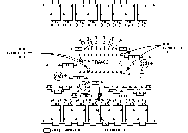
Figure 12: Suggested layout and component
placement for a TRA402 Evaluation Board.
Copyright© September 1995. LeCroy is a registered trademark of LeCroy Corporation. All rights reserved. Information in this publicaction supersedes all earlier versions.