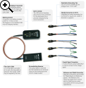
Key Features
-
150 MHz bandwidth
-
35 kV common-mode voltage rating
-
Silicon Carbide Suitable
-
Superior Noise and Rejection
-
160 dB CMRR
-
Low loop inductance
-
Low attenuation
-
Reduced DUT loading, better pulse response compared to conventional HV differential probes
-
Selectable tips for from +/-1V to +/-40V

Silicon Carbide Suitable
The new HVFO108, with 150 MHz of bandwidth, is perfect for device research engineers designing Silicon and Silicon Carbide devices, and system development engineers incorporating Silicon Carbide devices.
Upper-side Gate Drive Signal Measurements

The HVFO108 faithfully reproduces upper-side gate drive signals without loading and distortion, allowing a clear view of the Miller effect. Any conventional HV differential probe with high tip capacitance in parallel with CGE or CGS, and/or high impedance and large loop inductance in series with the gate drive impedance will at best load the gate drive signal or pick up interference and at worst cause circuit malfunction. The HVFO108 performs much better for these measurements.
Floating Control or Sensor Signal Measurements

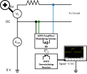
The HVFO108 measures only the low voltage sensor voltage across its high impedance input leads. Total load on the device under test (DUT) is very small. Furthermore, the low lead loop inductance, >100dB CMRR, and low attenuation provide superior signal fidelity, noise and rejection.
EMC, EFT, ESD and RF Immunity Testing and System Optimization
AC and DC sensor signals floating at a high voltage or in the presence of EMC disturbance signals can be acquired with high signal fidelity and correctly correlated to in-circuit and control activities.
Optical Isolation is Best

Optical isolation between the probe tip and the oscilloscope input reduces adverse loading of the DUT, provides faithful pulse response, and increases confidence in the measurement. Safety against dangerous high voltage levels can be ensured and unsafe "floating" of the oscilloscope can be avoided.
Superior Noise and Rejection
High CMRR (140 dB) provides more accurate representation of the measured signal despite the presence of high dV/dt or dA/dt events elsewhere in the circuit. The test lead is optimized to limit loop inductance and radiated pickup. Tip attenuations are optimized for a wide range of signal amplitudes.